Metal-bonded light emitting diode and method for forming metal-bonded light emitting diode

A technology of light-emitting diodes and metal bonds, which is applied to metal-bonded light-emitting diodes to form metal-bonded light-emitting diodes, can solve the problems of not considering the cost of various material characteristics, and achieve easy control, low cost, and low boiling point. Effect

Inactive Publication Date: 2017-11-14
TYNTEK
View PDF5 Cites 0 Cited by
  • Summary
  • Abstract
  • Description
  • Claims
  • Application Information

AI Technical Summary

Problems solved by technology

[0004] However, due to the above-mentioned method of using metal as the semiconductor material for bonding to form the light-emitting diode 1, it only uses a single metal material as the material of the bonding layer 14, and does not consider the characteristics and costs of various materials in the selection of materials. The problem of high and low, thus causing many problems in the use of material bonding

Method used


Image

  • Metal-bonded light emitting diode and method for forming metal-bonded light emitting diode
  • Metal-bonded light emitting diode and method for forming metal-bonded light emitting diode
  • Metal-bonded light emitting diode and method for forming metal-bonded light emitting diode

Examples


Embodiment Construction

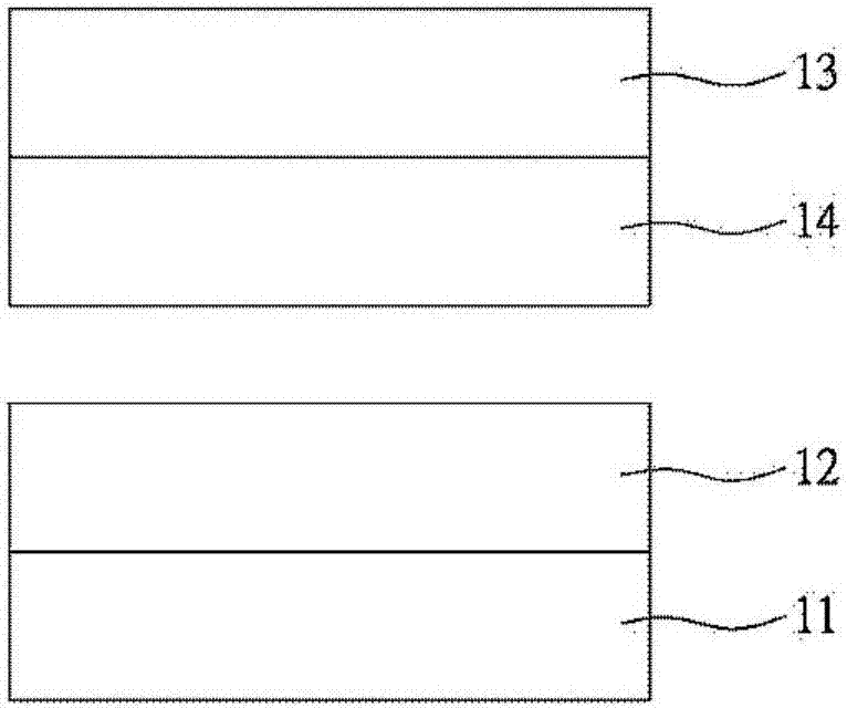
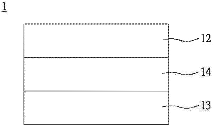
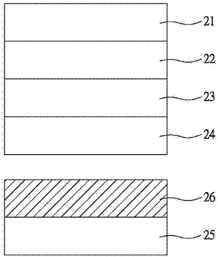
[0047] see Figure 2A and Figure 2B , which is a structural diagram completed by the method for forming a metal-bonded light-emitting diode according to the present invention. The method for forming a metal-bonded light-emitting diode of the present invention includes the following steps: setting a first substrate 25; forming a first bonding metal layer 26 on the first substrate 25; setting a second substrate 21; forming an epitaxial layer 22 on the second substrate 21 ; forming a conductive oxide layer 23 on the epitaxial layer 22 ; forming a second bonding metal layer 24 on the conductive oxide layer 23 ; bonding the first bonding metal layer 26 and the second bonding metal layer 24 ; removing the second substrate 21 .

[0048] see Figure 2C , which is a structural diagram of adding a covering layer according to the method for forming a metal bonded light-emitting diode of the present invention. The above method also includes forming a cover layer 27 between the epitaxi...


PUM


Abstract

The invention provides a metal-bonded light emitting diode, which comprises a substrate, a first bonding metal layer, a second bonding metal layer, a conductive oxide layer and an epitaxial layer. The first bonding metal layer is formed on the substrate. The second bonding metal layer is formed on the first bonding metal layer. The conductive oxide layer is formed on the second bonding metal layer. The epitaxial layer is formed on the conductive oxide layer. The invention further comprises a method for forming the metal-bonded light emitting diode, and the method comprises the steps of: setting a first substrate; forming the first bonding metal layer on the first substrate; setting a second substrate; forming the epitaxial layer on the second substrate; forming the conductive oxide layer on the epitaxial layer; forming the second bonding metal layer on the conductive oxide layer; bonding the first bonding metal layer and the second bonding metal layer; and removing the second substrate.

Description

technical field [0001] The invention belongs to a light-emitting diode, in particular to a metal-bonded light-emitting diode and a method for forming a metal-bonded light-emitting diode. Background technique [0002] Light emitting diodes are widely used products at present, and can be applied in various technical fields. However, in the technical field of light-emitting diodes, one of the most important issues at present is how to increase the brightness of the light-emitting diodes while reducing the manufacturing cost of the light-emitting diodes. [0003] As mentioned above, among the current technologies for improving the brightness of LEDs, one of them is to use metals as semiconductor materials for bonding to form LEDs. see Figure 1A and Figure 1B , which is a structure diagram of a light-emitting diode formed by utilizing metal bonding in the prior art. Further, the method of using metal as a bonding semiconductor material for forming a light-emitting diode is t...

Claims


Application Information

Patent Timeline
Patent Type & Authority Applications(China)
IPC IPC(8): H01L33/48H01L33/00
CPCH01L33/48H01L33/005
Inventor 龚正陈怡宏梁永隆
Owner TYNTEK
Why Eureka
Try Eureka