PCB apparent defect automatic detection system and method based on image

An automatic detection and defect detection technology, applied in the field of defect detection, can solve the problems of low detection efficiency and accuracy of PCB boards, high price, and high false detection rate, and achieve the goal of reducing hardware control costs, reducing defect rates, and low false detection rates. Effect

Inactive Publication Date: 2017-11-24
NORTHWESTERN POLYTECHNICAL UNIV
View PDF1 Cites 130 Cited by
  • Summary
  • Abstract
  • Description
  • Claims
  • Application Information

AI Technical Summary

Problems solved by technology

Manual visual inspection mainly has shortcomings such as low efficiency and high false detection rate. Electronic detection is a contact detection. The detection sensor is in direct contact with the detected object, and there is a risk of failure due to physical contact, and the detection efficiency of the increasingly dense PCB board with lower precision
At present, the automatic detection technology of PCB apparent defects is relatively mature in foreign countries, and there are already equipments with relatively good detection effects, but the price is expensive; there are also some researches on this in China, and defect detection methods such as defect detection methods based on morphology, Defect detection methods based on image fusion, etc., but most of them still have accuracy problems, so it is very important to speed up the pace of domestic research

Method used


Image

  • PCB apparent defect automatic detection system and method based on image
  • PCB apparent defect automatic detection system and method based on image
  • PCB apparent defect automatic detection system and method based on image

Examples


Embodiment Construction

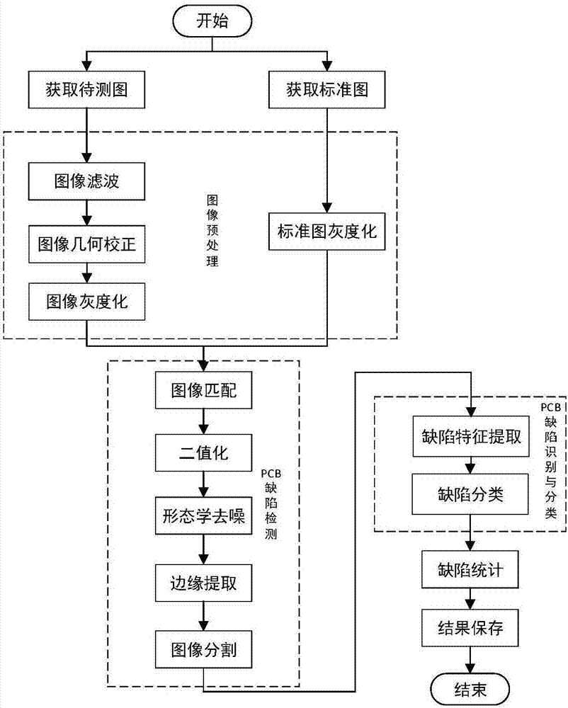
[0039]The present invention will be further described below in conjunction with the accompanying drawings and embodiments, and the present invention includes but not limited to the following embodiments.

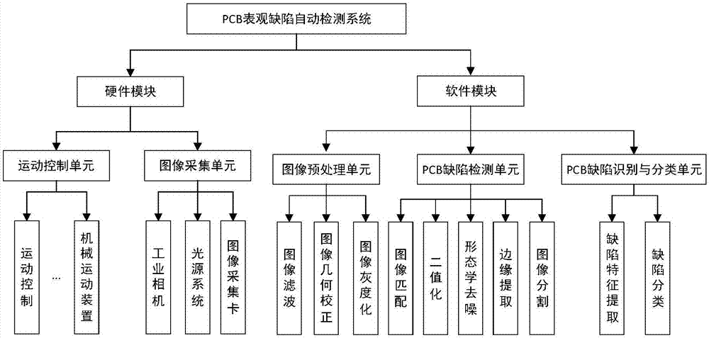
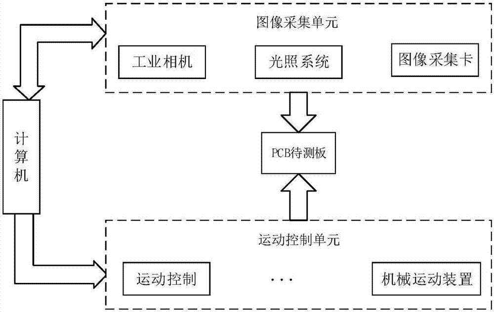
[0040] The image-based PCB apparent defect automatic detection system provided by the present invention includes a motion control unit, an image acquisition unit, an image preprocessing unit, a PCB defect detection unit, and a PCB defect identification and classification unit, wherein:

[0041] The motion control unit is used to transfer the PCB to be tested to the designated position of the image acquisition unit through the transfer device;

[0042] The image acquisition unit is used to obtain the PCB to-be-tested image and the PCB standard image by using the image acquisition card, the light source system and the industrial camera;

[0043] The image preprocessing unit is used to perform image filtering, image correction, and image grayscale preprocessing operations on th...


PUM


Abstract

The invention provides a PCB apparent defect automatic detection system and method based on an image and aims at solving the problems that detection efficiency is low and misjudgment rate is high. The method comprises the following steps: firstly transmitting a to-be-detected PCB to a specified position by virtue of a motion control unit; acquiring an image of the to-be-detected PCB by utilizing image acquisition equipment such as an image acquisition card and an industrial camera; then sequentially carrying out a series of operation such as image preprocessing, PCB defect detection and PCB defect identification and classification on the acquired image, so that PCB defect automatic detection is completed; and finally realizing real-time automatic sorting of an unqualified PCB and timely reporting a defect position and a defect analysis result to an operator. The system and method which are provided by the invention can automatically detect the PCB defect and identify the defect type to a great extent, and false detection rate is reduced, so that enterprise cost is reduced, and the system and method which are provided by the invention have stronger practicability.

Description

technical field [0001] The invention relates to the technical field of defect detection, in particular to the automatic detection of PCB apparent defects, including detection and identification of missing welding and wrong welding of components in a PCB board with components. Background technique [0002] As one of the key development directions of electronic information industry and intelligent manufacturing industry, PCB's reliability has important research value. At present, the quality inspection for PCB mainly includes traditional manual visual inspection and electronic inspection, among which electronic inspection is divided into needle bed inspection and flying probe inspection. Manual visual inspection mainly has shortcomings such as low efficiency and high false detection rate. Electronic detection is a contact detection. The detection sensor is in direct contact with the detected object, and there is a risk of failure due to physical contact, and the detection effi...

Claims


Application Information

Patent Timeline
Patent Type & Authority Applications(China)
IPC IPC(8): G01N21/956G01N21/88G06T7/00G06K9/62
CPCG06T7/001G01N21/8851G01N21/95607G01N2021/95646G01N2021/8874G01N2021/8887G06T2207/30141G06F18/2411
Inventor 郭阳明刘珊米琪孙利马捷中朱培灿林鹏
Owner NORTHWESTERN POLYTECHNICAL UNIV
Why Eureka
Try Eureka