GaN HEMTs power device-to-diamond heat sink transfer method

A technology of power device and transfer method, which is applied in the manufacture of electric solid-state devices, semiconductor devices, semiconductor/solid-state devices, etc. It is difficult to meet the heat dissipation requirements of the device, and achieve the effect of avoiding damage, easy implementation, and good repeatability

Inactive Publication Date: 2017-11-24
XI AN JIAOTONG UNIV
View PDF2 Cites 6 Cited by
  • Summary
  • Abstract
  • Description
  • Claims
  • Application Information

AI Technical Summary

Problems solved by technology

[0003] The traditional solution to the heat dissipation of GaN HEMTs power devices is to prepare the device on a sapphire or SiC substrate and use the sapphire or SiC substrate to dissipate heat. However, sapphire and SiC have limited thermal conductivity (sapphire thermal conductivity 35W / m K, SiC The thermal conductivity of 490W / m K) is difficult to meet the heat dissipation requirements of high-frequency and high-power applications, because the preparation of large-scale high-quality diamond single crystal substrates is very difficult, and because there is a large lattice between GaN and diamond Mismatch and thermal mismatch, the epitaxial growth temperature is usually above 1000°C, it is very difficult to carry out GaN heteroepitaxy on a diamond substrate, and it is difficult for diamond materials to form a high-performance heterostructure

Method used


Image

  • GaN HEMTs power device-to-diamond heat sink transfer method
  • GaN HEMTs power device-to-diamond heat sink transfer method
  • GaN HEMTs power device-to-diamond heat sink transfer method

Examples


Embodiment

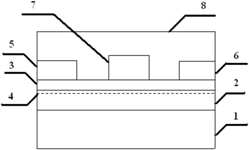
[0045] Such as figure 1 As shown, the sapphire substrate GaN HEMTs power device, the device structure is a common structure, the thickness of the sapphire substrate 1 is 500μm, the thickness of the undoped GaN layer 2 is 3um, the thickness of the AlGaN barrier layer 3 is 20nm, the source electrode 5 and the drain electrode 6 are ohm The contact electrode adopts Ti / Al / Ti / Au (20 / 100 / 40 / 55nm) multi-layer metal structure, the gate 7 is a Schottky contact electrode adopts Ni / Au / (30 / 250nm) two-layer metal structure, the gate The distance between 7 and source 5 is 2.5 μm, the distance between gate 7 and drain 6 is 2.5 μm, the length of gate 7 is 3 μm, and the width of gate 7 is Wg=100 μm;

[0046] Fabrication of GaN HEMTs power devices on sapphire substrates includes the following steps:

[0047] (1), first clean the sapphire substrate 1, use carbon trichloride, tetrachlorethylene, acetone, ethanol, and deionized water to ultrasonicate for 5 minutes each, and then blow dry in nitrog...


PUM


Abstract

A GaN HEMTs power device-to-diamond heat sink transfer method disclosed by the present invention comprises the steps of growing a GaN HEMTs power device on a sapphire substrate, then adopting a Si wafer as a temporary supporting material to grow on the GaN HEMTs power device, and then separating the sapphire substrate from the GaN HEMTs power device, and adhering the Si wafer to the GaN HEMTs power device via a thermoplastic adhesive, and finally peeling the Si wafer on the GaN HEMTs power device, thereby obtaining the diamond heat sink wafer GaN HEMTs power device. By adopting the diamond of high thermal conductivity as a heat sink wafer of the GaN HEMTs power device, the heat radiation capability of the GaN HEMTs power device at the high-frequency and large-power application is improved substantially, and by adopting a low-temperature bonding method to adhere the heat radiation problem of the GaN HEMTs power device at the high-frequency and large-power application and the diamond heat sink wafer, the damage of the conventional high-temperature bonding to the performances of the device is avoided effectively. The transfer method of the present invention is simple in technology and good in repeatability, and is easy to realize.

Description

technical field [0001] The invention relates to the technical field of heat dissipation of GaN HEMTs power devices, in particular to a method for transferring GaN HEMTs power devices to diamond heat sinks. Background technique [0002] As a typical power semiconductor device, GaN HEMTs have the advantages of high voltage resistance, high current, high power, and high temperature resistance, and are a very promising power electronic device. However, as the output power of the device continues to increase, the heat generated by the device will increase sharply. If the heat is not dissipated in time, the high temperature generated by the heat inside the device will seriously affect the performance of the device. Therefore, heat dissipation has become an urgent issue in the design and manufacture of GaN HEMTs power devices. [0003] The traditional solution to the heat dissipation of GaN HEMTs power devices is to prepare the device on a sapphire or SiC substrate and use the sap...

Claims


Application Information

Patent Timeline
Patent Type & Authority Applications(China)
IPC IPC(8): H01L21/683H01L21/335H01L23/367H01L23/373
CPCH01L21/6835H01L23/3672H01L23/3732H01L29/66462H01L2221/68368H01L2221/68386
Inventor 张景文王进军陈旭东翟文博王晓亮卜忍安王宏兴侯洵
Owner XI AN JIAOTONG UNIV
Why Eureka
Try Eureka