Low-temperature microwave source, low-temperature microwave source chip and manufacture method thereof

A microwave source and low-temperature technology, which is applied in the manufacture/processing of superconductor devices, devices containing a node of different materials, superconducting devices, etc., can solve the needs that microwave signals cannot reach solid-state quantum chip control and quantum computing , loud noise, etc.

Active Publication Date: 2017-11-24
UNIV OF SCI & TECH OF CHINA
View PDF5 Cites 11 Cited by
  • Summary
  • Abstract
  • Description
  • Claims
  • Application Information

AI Technical Summary

Problems solved by technology

However, in the prior art, the measurement techniques used to control qubits are all performed by classical instruments. For example, the microwave source used to control qubits is difficult to meet the current needs of solid-state quantum chip control and quantum computing.
[0003] In the prior art, the microwave source used to manipulate qubits has the problem of high noise on the one hand, and on the other hand, because the microwave source is applied through the room temperature line, before the microwave signal goes from room temperature to the ultra-low temperature quantum chip, it needs to be processed. Complex filtering, attenuation and other optimization design, but often the optimized microwave signal still cannot meet the requirements of solid-state quantum chip control and quantum computing

Method used


Image

  • Low-temperature microwave source, low-temperature microwave source chip and manufacture method thereof
  • Low-temperature microwave source, low-temperature microwave source chip and manufacture method thereof
  • Low-temperature microwave source, low-temperature microwave source chip and manufacture method thereof

Examples


Embodiment Construction

[0095] The following will clearly and completely describe the technical solutions in the embodiments of the present invention with reference to the accompanying drawings in the embodiments of the present invention. Obviously, the described embodiments are only some, not all, embodiments of the present invention. Based on the embodiments of the present invention, all other embodiments obtained by persons of ordinary skill in the art without making creative efforts belong to the protection scope of the present invention.

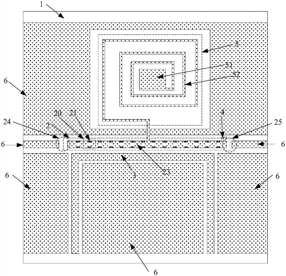
[0096] An embodiment of the present invention provides a low-temperature microwave source chip, specifically, as figure 1 As shown, it is a top view of the low-temperature microwave source chip, which includes a substrate 1 and a transmission cavity 2 on the surface of the substrate 1, a bias junction 4, a voltage bias line 5, and a DC bias line 3 .

[0097]Wherein, the substrate 1 is a semiconductor substrate, such as silicon or sapphire. Since the dielectr...


PUM


Abstract

The invention discloses a low-temperature microwave source, a low-temperature microwave source chip and a manufacture method thereof. The chip comprises a substrate, a transmission cavity, a bias junction, a voltage bias line and a direct current bias line, wherein the transmission cavity, the bias junction, the voltage bias line and the direct current bias line are located on the surface of the substrate. The transmission cavity comprises a SQUID chain and is used for emitting microwave photons. The bias junction is electrically connected with the transmission cavity and is used for generating microwave photons. The voltage bias line is used for applying bias voltage to the bias junction, so that electronic cooper pairs in the bias junction are transformed into microwave photons through stimulated emission. The direct current bias line is used for applying a magnetic field to the transmission cavity. The resonant frequency of the transmission cavity is determined by the total capacitance and total inductance of the SQUID chain. The total inductance of the SQUID chain varies with the size of the magnetic field. The size of the magnetic field varies with the magnitude of the current in the direct current bias line. According to the invention, the low-temperature microwave source chip generates microwave photons through stimulated emission; the stability of the frequency, the amplitude and the phase of emitted microwave photons is ensured; and microwave source requirements are met.

Description

technical field [0001] The invention relates to microwave circuit components, more specifically, to a low-temperature microwave source, a low-temperature microwave source chip and a manufacturing method thereof. Background technique [0002] In the field of solid-state quantum computing, only by placing the quantum chip in an extremely low temperature environment can the quantum characteristics of the qubit be fully highlighted, and it is also necessary to suppress the influence of environmental noise on quantum coherence. However, in the prior art, the measurement techniques used to control qubits are all performed by classical instruments. For example, the microwave source used to control qubits is difficult to meet the current needs of solid-state quantum chip control and quantum computing. [0003] In the prior art, the microwave source used to manipulate qubits has the problem of high noise on the one hand, and on the other hand, because the microwave source is applied ...

Claims


Application Information

Patent Timeline
Patent Type & Authority Applications(China)
IPC IPC(8): H01L27/18H01L39/22H01L39/24
CPCH10N69/00H10N60/12H10N60/0912
Inventor 郭国平段鹏孔伟成贾志龙薛光明郭光灿
Owner UNIV OF SCI & TECH OF CHINA
Why Eureka
Try Eureka