Antenna array

A technology of antenna elements and dielectric boards, which is applied in the field of communication, can solve problems such as the need to ensure isolation, narrow bandwidth, and low antenna signal gain, and achieve the effects of improving communication index performance, best broadband performance, and improving applicability

Active Publication Date: 2017-11-24
CHENGDU T-RAY TECH CO LTD
View PDF4 Cites 4 Cited by
  • Summary
  • Abstract
  • Description
  • Claims
  • Application Information

AI Technical Summary

Problems solved by technology

[0004] The present application provides an antenna array element, which is used to solve the antenna array element in the large antenna array existing in the prior art or the antenna signal gain is very low due to the need to achieve a better broadband range, or the need to ensure isolation Technical issues causing narrow bandwidth

Method used


Image

  • Antenna array
  • Antenna array
  • Antenna array

Examples


Embodiment 1

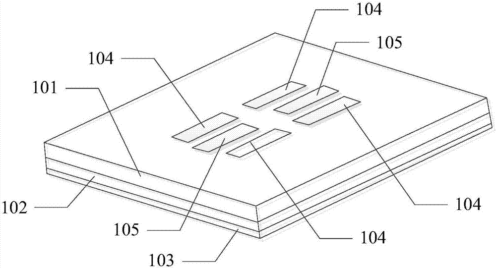
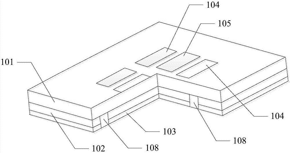
[0034] Please refer to figure 1 , figure 2 , image 3 , Figure 4 , Figure 5 ,and Image 6 , Embodiment 1 of the present application provides an antenna array element, including:

[0035] The first substrate layer 101 includes a first dielectric plate and a first metal layer 1011 attached to the surface of the first dielectric plate;

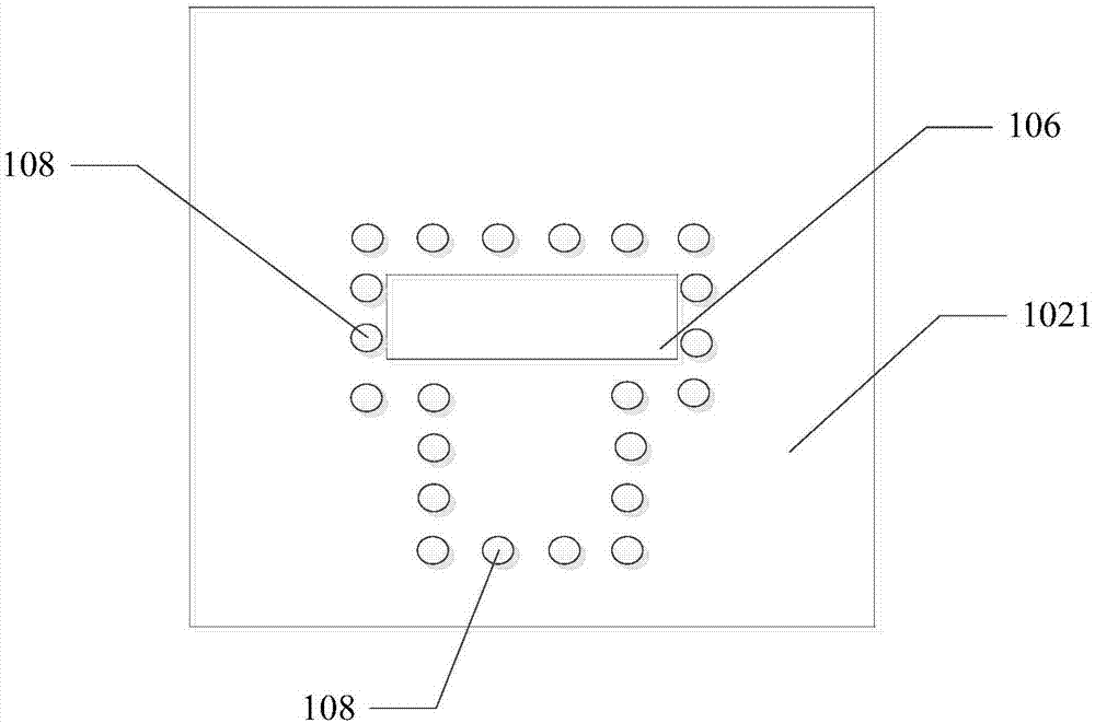
[0036] The second substrate layer 102 includes a second dielectric board and a first metal layer 1011 attached to the surface of the second dielectric board, and the second metal layer 1021 is attached to the first dielectric board;

[0037] The third substrate layer 103 includes a third dielectric board and a third metal layer 1031 attached to the surface of the third dielectric board, and the third metal layer 1031 is attached to the second dielectric board;

[0038] The first radiating patch group and the second radiating patch group are attached on the surface of the first metal layer 1011 and are opposite to the first dielectric pla...


PUM


Abstract

The invention discloses an antenna array, by setting three substrate layers, attaching patches with different sizes to a first metal layer surface in a first substrate layer, setting a coupling slot at a metal layer in a second substrate layer, setting a feed microstrip as a metal layer in a third substrate layer, and setting at least one metal through hole which surrounds the feed microstrip in the second substrate layer and the third substrate layer, so the antenna array of the embodiment of the invention has high isolation and better broadband performance, and the antenna array has the advantages that various communication performance indexes of the antenna array is improved, the applicability of a large antenna array is improved, and the high integration of the large antenna array is ensured.

Description

technical field [0001] The invention relates to the technical field of communications, in particular to an antenna array element. Background technique [0002] At present, in order to achieve high integration, the traditional large-scale antenna array usually adopts a simple form of probe-fed patch antenna element. The patch of this form of antenna element is mostly rectangular or circular, and its bandwidth is very narrow. Usually Only 1% to 7%. In the prior art, in order to make the antenna element have a wider bandwidth, a layer of parasitic patch is usually added on the radiation patch of the antenna element in the above form, but this kind of structure has a large loss of signal strength, and the antenna Signal gain is very low. Another existing way to increase the antenna bandwidth is to use slot coupling feeding. However, when this method is applied to the elements of a large antenna array, due to the strong coupling between the antenna elements, it is necessary to ...

Claims


Application Information

Patent Timeline
Patent Type & Authority Applications(China)
IPC IPC(8): H01Q1/38H01Q1/52H01Q13/10
Inventor 郭凡玉陈智慧赵国华胡荣颜微赵学文向茂
Owner CHENGDU T-RAY TECH CO LTD
Why Eureka
Try Eureka