Bias Circuit and Low Noise Amplifier

A low-noise amplifier, bias circuit technology, applied in amplifiers, improving amplifiers to reduce noise effects, electrical components, etc., can solve the problems of low reliability of low-noise amplifiers, and achieve the effect of improving reliability and overcoming low reliability.

Active Publication Date: 2020-09-11
上海韦玏微电子有限公司 +1
View PDF4 Cites 0 Cited by
  • Summary
  • Abstract
  • Description
  • Claims
  • Application Information

AI Technical Summary

Problems solved by technology

[0004] The technical problem to be solved by the present invention is to overcome the defect of low reliability when the low noise amplifier works in the off mode in the prior art, and provide a bias circuit and a low noise amplifier that can improve the reliability of the low noise amplifier in the off mode. noise amplifier

Method used


Image

  • Bias Circuit and Low Noise Amplifier
  • Bias Circuit and Low Noise Amplifier

Examples


Embodiment 1

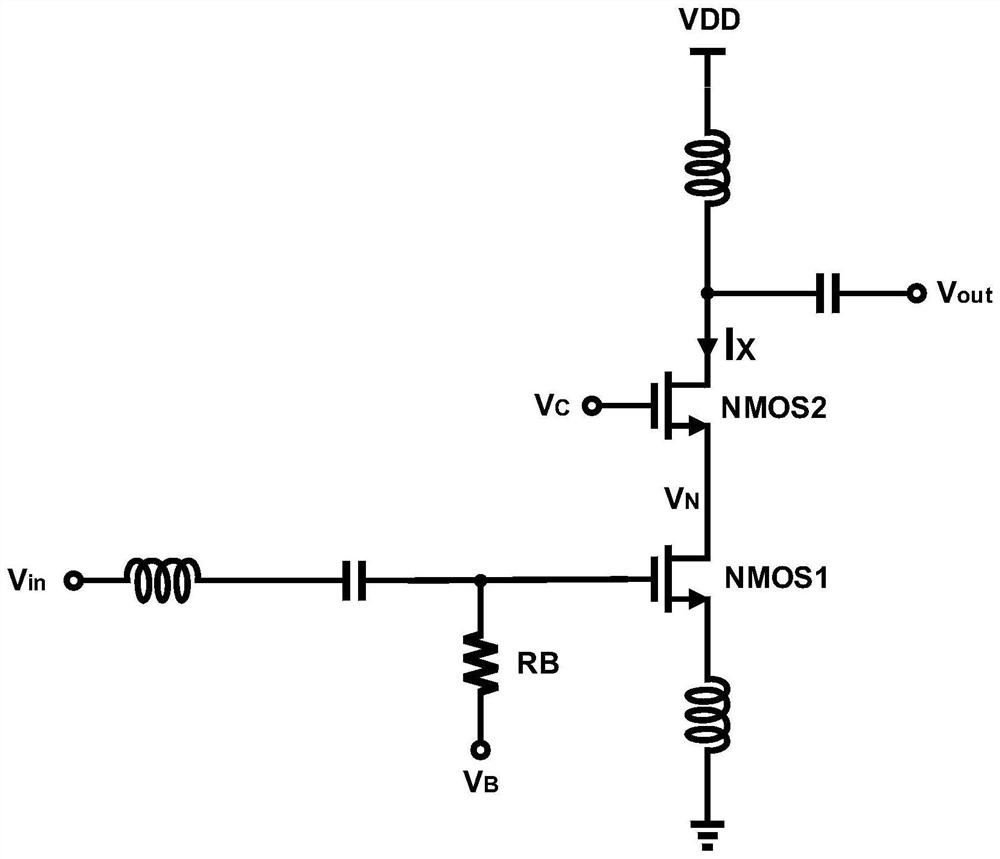
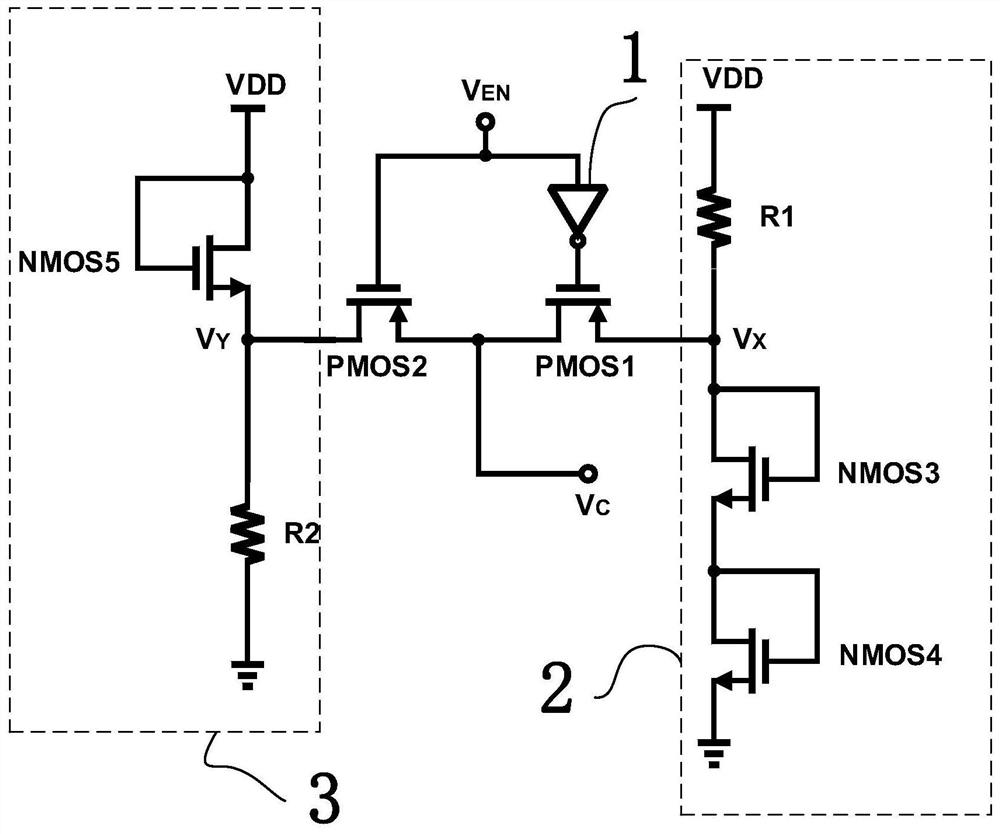
[0023] Such as figure 2 As shown, a bias circuit for figure 1 The traditional low noise amplifier shown includes an inverter 1, a first switching tube PMOS1, a second switching tube PMOS2, a first bias voltage generating circuit 2 and a second bias voltage generating circuit 3, and the first switching tube PMOS1 The source is connected to the first bias voltage V X , the drain of the second switching transistor PMOS2 is connected to the second bias voltage V Y , the drain of the first switch PMOS1 and the source of the second switch PMOS2 are connected to the voltage output terminal V C ; The grid of the first switching tube PMOS1 is electrically connected to the output terminal of the inverter 1, and the input terminal of the inverter 1 and the grid of the second switching tube PMOS2 are connected to the control voltage V EN ;Voltage output terminal V C for output bias voltage to figure 1 The gate of the common-gate transistor NMOS2 is shown in a conventional LNA.

[0...

Embodiment 2

[0028] This embodiment provides a low noise amplifier, the low noise amplifier isfigure 1 The traditional LNA is based on the addition of figure 2 In the shown bias circuit, the voltage output end of the bias circuit is electrically connected to the gate of the common-gate transistor.


PUM


Abstract

The invention discloses a bias circuit and a low-noise amplifier, wherein the bias circuit includes a phase inverter, a first switch tube and a second switch tube; a first bias voltage is connected to a source of the first switch tube, a second bias voltage is connected to a drain of the second switch tube, and a drain of the first switch tube and a source of the second switch tube are connected to a voltage output end; a gate of the first switch tube is electrically connected to the output end of the phase inverter, and the input end of the phase inverter and a gate of the second switch tube are connected to a control voltage; the voltage output end is used for outputting bias voltages to gates of common-gate transistors of the low-noise amplifier. The bias circuit and the low-noise amplifier according to the invention have the advantages that the defect that the low-noise amplifier of the prior art has low reliability when operating in an off mode is overcome, and the reliability of the low-noise amplifier operating in the off mode is improved by providing different bias voltages to the gates of the common-gate transistors, having different operating modes, in the low-noise amplifier.

Description

technical field [0001] The invention relates to the technical field of integrated circuits, in particular to a bias circuit and a low-noise amplifier. Background technique [0002] Low-noise amplifiers are generally used as high-frequency or intermediate-frequency preamplifiers for various radio receivers, and amplifier circuits for high-sensitivity electronic detection equipment, and are especially widely used in mobile communication infrastructure, such as transceiver wireless communication cards, tower tops Amplifiers, combiners, repeaters, and remote / digital wireless broadband head-end equipment, etc. [0003] Traditional low noise amplifiers such as figure 1 As shown, the input voltage Vin and the output voltage Vout can work in two modes: amplification mode and shutdown mode. The voltage V across the resistor RB in amplified mode B is set to be greater than the threshold voltage of the transistor NMOS1 (N-type metal-oxide-semiconductor), at this time the current I ...

Claims


Application Information

Patent Timeline
Patent Type & Authority Patents(China)
IPC IPC(8): H03F1/26
CPCH03F1/26H03F2200/372
Inventor 李旋冯昊李小勇
Owner 上海韦玏微电子有限公司
Why Eureka
Try Eureka