Time control method and system for organic solderability preservatives (OSP) surface processing on printed circuit board (PCB)

A surface treatment and PCB board technology, applied in the secondary treatment of printed circuits, anti-corrosion parts, patterns and photolithography, etc., can solve the problems of loss, waste of human and financial resources, lax supervision and return to the factory, and save production costs , Improve work efficiency and reduce the effect of returning to the factory

Active Publication Date: 2017-11-28
ZHENGZHOU YUNHAI INFORMATION TECH CO LTD
View PDF3 Cites 2 Cited by
  • Summary
  • Abstract
  • Description
  • Claims
  • Application Information

AI Technical Summary

Problems solved by technology

In the existing technology, only manual supervision is used, which wastes human and financi...

Method used


Image

  • Time control method and system for organic solderability preservatives (OSP) surface processing on printed circuit board (PCB)
  • Time control method and system for organic solderability preservatives (OSP) surface processing on printed circuit board (PCB)

Examples


Embodiment Construction

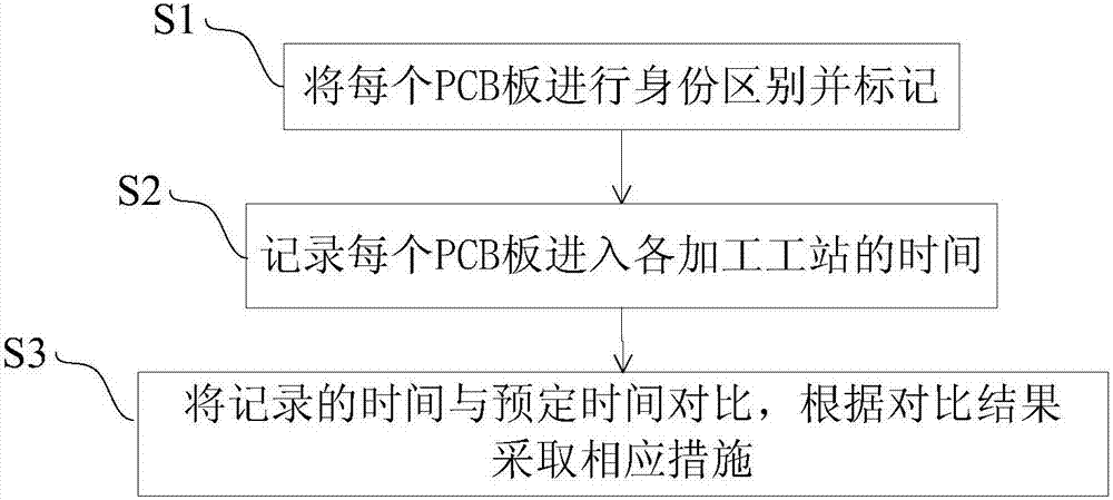
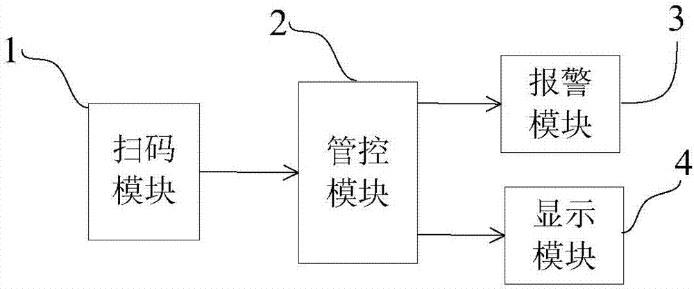
[0031] In order to clearly illustrate the technical features of this solution, the present invention will be described in detail below through specific implementation modes and in conjunction with the accompanying drawings. The following disclosure provides many different embodiments or examples for implementing different structures of the present invention. To simplify the disclosure of the present invention, components and arrangements of specific examples are described below. Furthermore, the present invention may repeat reference numerals and / or letters in different instances. This repetition is for the purpose of simplicity and clarity and does not in itself indicate a relationship between the various embodiments and / or arrangements discussed. It should be noted that components illustrated in the figures are not necessarily drawn to scale. Descriptions of well-known components and processing techniques and processes are omitted herein to avoid unnecessarily limiting the...


PUM


Abstract

The invention discloses a time control method and system for organic solderability preservatives (OSP) surface processing on a printed circuit board (PCB). The method comprises the steps of performing identification on each PCB, and marking each PCB; recording time of each PCB entering each processing station; and comparing recorded time with preset time, and taking corresponding measure according to a comparison result. The system comprises a scanning module, a control module, a warning module and a display module, wherein an output end of the scanning module is connected with an input end of the control module, and an output end of the control module is connected with the warning module and the display module. Compared with the prior art, the processing time of the PCB is strictly controlled, the quality of the PCB leaving from a factory is ensured, the return rate is greatly reduced, manual control is omitted, and the production cost is reduced.

Description

technical field [0001] The invention relates to the technical field of circuit board processing, in particular to a time control method and system for OSP surface treatment of PCBs. Background technique [0002] With the continuous development of electronic products in the direction of lightness, thinness, shortness, miniaturization and multi-function, PCB (Printed Circuit Board, printed circuit board) is also developing in the direction of high precision, thinness and multi-layer. In recent years, with the rapid development of surface mount technology, high-density PCB boards have continued to develop, making hot air leveling process welding less and less able to meet the needs of processing. At the same time, the tin-lead soldering material used in the hot air leveling process does not meet the environmental protection requirements. [0003] In 2006, the EU RoHS (Restriction of Hazardous Substances, a directive restricting the use of certain hazardous components in electr...

Claims


Application Information

Patent Timeline
IPC IPC(8): H05K3/28
CPCH05K3/282H05K2203/0562
Inventor 冯金星
Owner ZHENGZHOU YUNHAI INFORMATION TECH CO LTD
Why Eureka
Try Eureka