Unlock instant, AI-driven research and patent intelligence for your innovation.

Method for creating a semiconductor wafer having profiled doping and wafers and solar cell components having a profiled field, such as drift and back surface

A technology for semiconductors and solar collectors, applied in semiconductor devices, semiconductor/solid-state device manufacturing, electrical components, etc., to achieve the effects of promoting carrier collection, eliminating differential reflectors, and high efficiency

Active Publication Date: 2017-11-28
1366 TECH INC
View PDF9 Cites 1 Cited by
  • Summary
  • Abstract
  • Description
  • Claims
  • Application Information

AI Technical Summary

Problems solved by technology

The application of aluminum has disadvantages

Method used


Image

  • Method for creating a semiconductor wafer having profiled doping and wafers and solar cell components having a profiled field, such as drift and back surface
  • Method for creating a semiconductor wafer having profiled doping and wafers and solar cell components having a profiled field, such as drift and back surface
  • Method for creating a semiconductor wafer having profiled doping and wafers and solar cell components having a profiled field, such as drift and back surface

Examples


Embodiment Construction

[0032] As discussed above, typical semiconductor wafers for use in solar collectors have relatively thick sections in which the majority carriers are of one donor / acceptor type, eg typically p-type. Such wafers are formed and subsequently processed so that in the case of predominantly p-type wafers one side is doped to have the opposite donor / acceptor type, thus n-type majority carriers. For a typical wafer, the first portion will be essentially 180 microns the full thickness, while the other type of portion will only be about 0.5 microns thick. The junction between two parts is called a p / n junction. The following discussion mainly concerns a new method for preparing relatively thick sections, usually p-type sections. The methods discussed below will typically be used to create such wafers. After performing the method steps discussed herein, a p / n junction and opposite carrier type portion will be created on one surface. These methods can also be used to create thick, pred...


PUM


Abstract

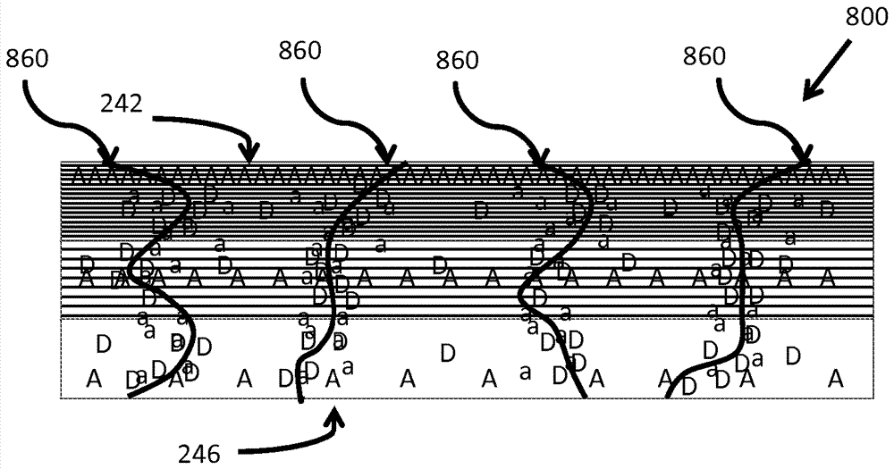
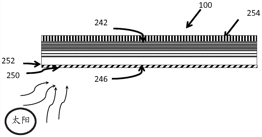
A semiconductor wafer forms on a mold containing a dopant. The dopant dopes a melt region adjacent the mold. There, dopant concentration is higher than in the melt bulk. A wafer starts solidifying. Dopant diffuses poorly in solid semiconductor. After a wafer starts solidifying, dopant cannot enter the melt. Afterwards, the concentration of dopant in the melt adjacent the wafer surface is less than what was present where the wafer began to form. New wafer regions grow from a melt region whose dopant concentration lessens over time. This establishes a dopant gradient in the wafer, with higher concentration adjacent the mold. The gradient can be tailored. A gradient gives rise to a field that can function as a drift or back surface field. Solar collectors can have open grid conductors and better optical reflectors on the back surface, made possible by the intrinsic back surface field.

Description

[0001] Related literature [0002] HEREBY CLAIMING THE PROTECTION OF METHODS OF CREATING ASEMICONDUCTOR WAFER HAVING A DRIFT FIELD WITH PROFILED DOPING AND WAFERSHAVING A PROFILED DRIFT FIELD, filed January 26, 2015, inventors Ralf Jonczyk et al., applicants Bedford, Massachusetts US Provisional Application No. 62 / 107,711 of priority to 1366 Technologies, Inc. of Germany, the entire disclosure of which is hereby incorporated by reference. Accordingly, protection is also claimed for the invention filed on October 8, 2015, entitled "METHODS FORCREATING A SEMICONDUCTOR WAFER HAVING PROFILED DOPING AND WAFERS AND SOLARCELL COMPONENTS HAVING A PROFILED FIELD, SUCH AS DRIFT AND BACK SURFACE", the inventors are Ralf Jonczyk, etc., The applicant is the priority of US Provisional Application No. 62 / 239,115 to 1366 Technologies, Inc. of Bedford, MA, the entire disclosure of which is also hereby incorporated by reference. Background technique [0003] The technique disclosed in U.S. Pat...

Claims


Application Information

Patent Timeline
Patent Type & Authority Applications(China)
IPC IPC(8): H01L21/00
CPCH01L21/00Y02E10/547H01L31/022425H01L31/068Y02E10/52C30B29/06H01L31/182C30B28/04C30B19/12C30B35/002C30B31/04C30B11/002C30B31/02Y02E10/546H01L31/1804Y02E10/544Y02P70/50H01L31/02167H01L31/0288H01L31/03046H01L31/048H01L31/06H01L31/18H01L31/056
Inventor R.荣茨克B.D.克南G.D.S.赫德尔森A.M.罗伦斯E.M.萨赫斯
Owner 1366 TECH INC