
Touch display device

A technology of touch display device and touch layer, which is applied in the fields of optics, instrumentation, electrical digital data processing, etc., and can solve the problems of affecting touch sensitivity, unfavorable touch position determination, high impedance, etc.

Active Publication Date: 2017-12-01
KUSN INFOVISION OPTOELECTRONICS
View PDF5 Cites 6 Cited by
  • Summary
  • Abstract
  • Description
  • Claims
  • Application Information

AI Technical Summary

Problems solved by technology

When the parasitic capacitance is large, it will interfere with the detection signal, which is not conducive to the determination of the touch position
In addition, due to the high impedance of the ITO electrode, the touch signal is attenuated, which affects the touch sensitivity. Different ITO film thicknesses have different chromatic aberrations and differences in transmittance, which affect the display.

Method used


Image

  • Touch display device
  • Touch display device
  • Touch display device

Examples


Embodiment Construction

[0032] Hereinafter, the present invention will be described in more detail with reference to the accompanying drawings. In the various figures, identical elements are indicated with similar reference numerals. For the sake of clarity, various parts in the drawings have not been drawn to scale. In addition, wirings other than the corresponding driving electrodes and sensing electrodes are not drawn in the figure, and some well-known parts may not be shown.

[0033] In the following, many specific details of the present invention are described, such as device structures, materials, dimensions, processing techniques and techniques, for a clearer understanding of the present invention. However, the invention may be practiced without these specific details, as will be understood by those skilled in the art.

[0034] Hereinafter, the present invention will be described in detail with reference to the accompanying drawings.

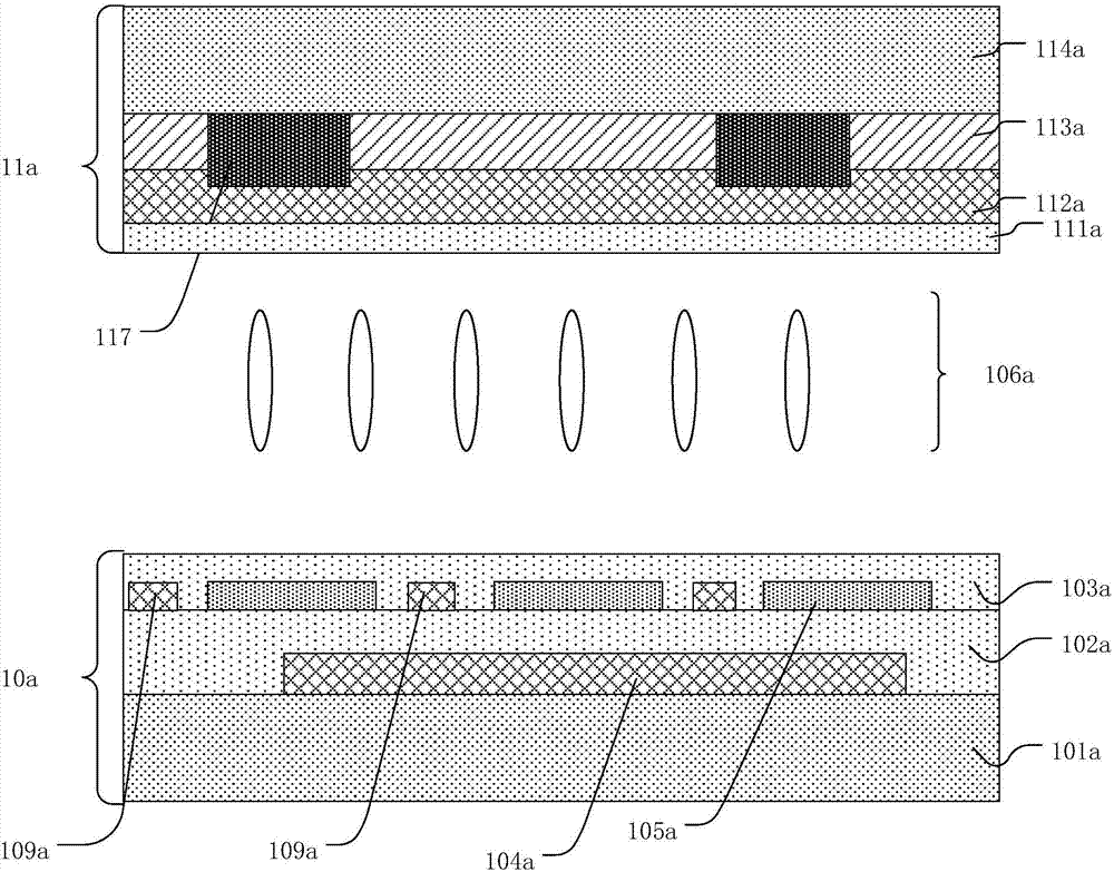
[0035] Figure 1a It is a schematic cross-sectional str...


PUM

PropertyMeasurementUnit
Line widthaaaaaaaaaa

Abstract

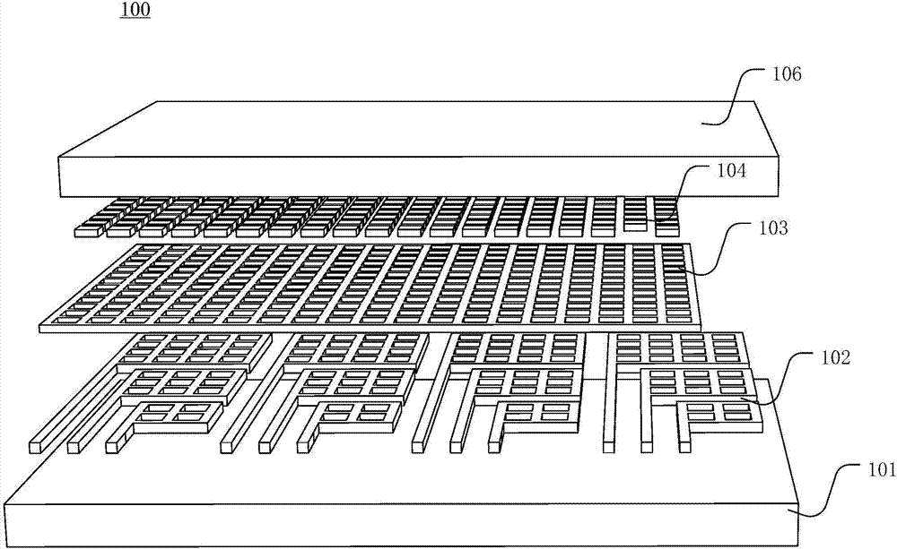
The present invention relates to the technical field of touch control, and in particular, to a touch display device. The touch display device comprises: a color filter substrate; an array substrate opposite to the color filter substrate; a liquid crystal layer arranged between the color filter substrate and the array substrate; and a touch layer including a plurality of electrode groups for detecting touch. The plurality of electrode groups are arranged on the color filter substrate or the array substrate; each of the electrode groups comprises a plurality of electrodes; each electrode in the plurality of electrode groups comprises a grid structure and electrode leads connected with the grid structure; and in each of the electrode groups, the electrode size gradually decreases in at least one direction, so that the space for electrode lead extension is provided. The design can effectively reduce the dead zone area, and change the dead zone shape, so that the user experience is improved.

Description

technical field [0001] The present invention relates to the technical field of touch control, in particular to a touch display device. Background technique [0002] Liquid crystal display devices have been widely used in mobile terminals such as cell phones and large-sized display panels such as flat TVs. A liquid crystal display device includes an array substrate, a color filter substrate and a liquid crystal layer sandwiched therebetween. The pixel electrode and the common electrode are formed on the substrate, and the rotation of the liquid crystal molecules of the liquid crystal layer is controlled by applying a driving voltage between them, thereby changing the light transmittance. [0003] Embedding a touch panel in a liquid crystal display device can further form a touch display panel. The touch display panel can not only provide a display function, but also provide a user interaction function. The integration of the two can reduce the total cost of electronic prod...

Claims


Application Information

Patent Timeline
IPC IPC(8): G06F3/041G06F3/044G02F1/1333G02F1/1343
CPCG02F1/13338G02F1/134309G06F3/0412G06F3/044
Inventor 邱峰青刘永锋陈敏
Owner KUSN INFOVISION OPTOELECTRONICS
Learn More