Graphene two-dimensional material protective layer-based topological insulator array photoelectric detector and preparation method and application thereof

A topological insulator and photodetector technology, applied in the field of photoelectric detection, can solve the problems of surface lattice structure damage, increase the difficulty of topological insulators, and affect the compatibility of topological insulator micro-nano processing technology, etc.

Active Publication Date: 2017-12-01
NAT UNIV OF DEFENSE TECH
View PDF5 Cites 15 Cited by
  • Summary
  • Abstract
  • Description
  • Claims
  • Application Information

AI Technical Summary

Problems solved by technology

[0004] Experiments have found that topological insulator thin films are easily affected by chemical reagents such as acetone, isopropanol, and developer, and the surface lattice structure is destroyed, and the inherent excellent properties of topological insulators are severely damaged.
This disadvantage seriously affects the compatibility of topological insulators with existing micro-nano processing techniques, and increases the difficulty of topological insulators entering practical applications.

Method used


Image

  • Graphene two-dimensional material protective layer-based topological insulator array photoelectric detector and preparation method and application thereof
  • Graphene two-dimensional material protective layer-based topological insulator array photoelectric detector and preparation method and application thereof
  • Graphene two-dimensional material protective layer-based topological insulator array photoelectric detector and preparation method and application thereof

Examples


Embodiment 1

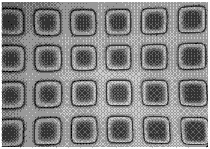
[0052] A topological insulator array photodetector based on a graphene-like two-dimensional material protective layer of the present invention, the photodetector includes a substrate, a topological insulator film, a single layer of graphene and an ITO transparent array electrode from bottom to top, wherein Single-layer graphene can also be the protective layer of other graphene-like two-dimensional materials. There is no topological insulator film and graphene-like two-dimensional material protective layer in the gap between the array units of the ITO transparent array electrode (that is, the two-layer structure is only provided under the array unit), and the doping of the topological insulator film and the substrate The type is reversed.

[0053] A kind of preparation method of the topological insulator array type photodetector based on graphene class two-dimensional material protective layer of above-mentioned present embodiment, comprises the following steps:

[0054] (1) ...


PUM

PropertyMeasurementUnit
concentrationaaaaaaaaaa

Abstract

The invention discloses a graphene two-dimensional material protective layer-based topological insulator array photoelectric detector and a preparation method and application thereof. The method comprises the following preparation process of (1) growing a topological insulator film which is opposite to a substrate in doping type on the substrate; (2) obtaining a graphene two-dimensional material protective layer/PMMA stack structure by adopting a wetting transfer method and transferring the graphene two-dimensional material protective layer/PMMA stack structure to the topological insulator film; (3) preparing an ITO array electrode through photoetching and magnetron sputtering; and (4) etching away the topological insulator film between array elements of the ITO array electrode and a graphene two-dimensional material through photoetching and reactive ion etching to obtain the photoelectric detector. According to the method, a topological insulator can be effectively prevented from being in direct contact with an organic liquid to be damaged, the method can be compatible with a traditional micro-nano technology, the dimension of the unit detector is shortened, the integration level is improved, a wide spectrum and an ultra-fast photoelectric response are obtained and the method has a wide application prospect.

Description

technical field [0001] The invention belongs to the technical field of photoelectric detection, and relates to a preparation method of a large-area topological insulator thin film photodetector, in particular to a topological insulator array photodetector based on a graphene-like two-dimensional material protective layer and its preparation method and application. Background technique [0002] With the continuous development of photodetection technology, traditional photodetectors are facing many problems such as insufficient wide response spectrum, insufficient response speed, mid-to-far infrared detectors must work in low temperature environment, and complex preparation process of photoelectric detection materials. In order to further promote the continuous development of photodetection technology, researchers at home and abroad have always regarded the search for new photodetection materials as the most important technical route for the development of a new generation of ...

Claims


Application Information

Patent Timeline
Patent Type & Authority Applications(China)
IPC IPC(8): H01L31/028H01L31/0352H01L31/10H01L31/18
CPCH01L31/028H01L31/035272H01L31/10H01L31/18Y02P70/50
Inventor 孙红辉池雅庆江天方粮
Owner NAT UNIV OF DEFENSE TECH
Why Eureka
Try Eureka