Mass transfer method of Micro LED (Light Emitting Diode) chips

A technology of light-emitting diodes and chips, which is applied in the directions of printed circuits, printed circuits, and electrical components connected with non-printed electrical components, can solve the problems of waste, low yield, and high production cost of MicroLED chips, and achieves mass transfer, The effect of reducing production costs and improving production efficiency

Active Publication Date: 2017-12-01
HC SEMITEK ZHEJIANG CO LTD
View PDF7 Cites 86 Cited by
  • Summary
  • Abstract
  • Description
  • Claims
  • Application Information

AI Technical Summary

Problems solved by technology

[0005] As long as one of the chips formed on the wafer has a defect, all the chips on the wafer will be replaced, causing a lot of waste, and the yield is very low, which greatly reduces the production efficiency of Micro LED chips, making Micro LED chips are expensive to produce

Method used


Image

  • Mass transfer method of Micro LED (Light Emitting Diode) chips
  • Mass transfer method of Micro LED (Light Emitting Diode) chips
  • Mass transfer method of Micro LED (Light Emitting Diode) chips

Examples


Embodiment

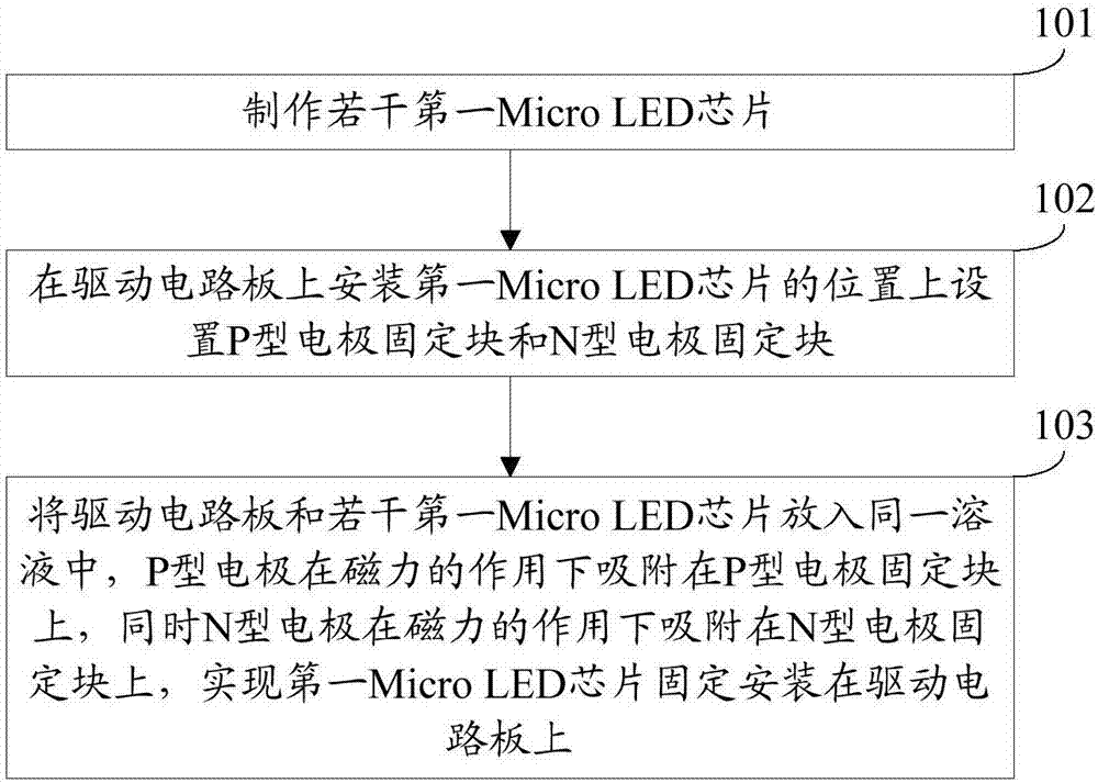
[0054] The embodiment of the present invention provides a method for mass transfer of Micro LED chips, see figure 1 , the method includes:

[0055] Step 101: Fabricate a number of first Micro LED chips.

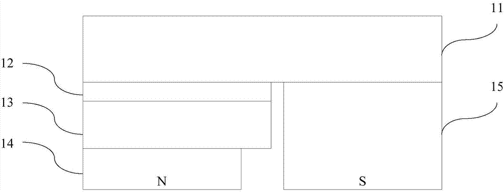
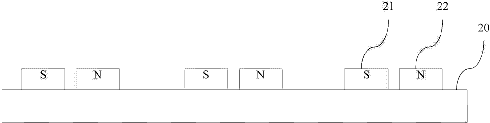
[0056] In this embodiment, the first Micro LED chip includes an N-type layer, a light-emitting layer, a P-type layer, a P-type electrode, and an N-type electrode. The N-type layer, the light-emitting layer, and the P-type layer are stacked in sequence. The groove extending to the N-type layer, the N-type electrode is arranged on the N-type layer in the groove, the P-type electrode is arranged on the P-type layer, the P-type electrode and the N-type electrode are magnets, and the P-type electrode is far away from the P-type layer One end of the N-type electrode and the end of the N-type electrode away from the N-type layer are heteronym magnetic poles.

[0057] Specifically, the maximum distance between two points on the cross section of the first Micro LED chip perpendicula...


PUM


Abstract

The invention discloses a mass transfer method of Micro LED (Light Emitting Diode) chips, and belongs to the technical field of a semiconductor. The mass transfer method comprises the steps of: producing a plurality of first Micro LED chips, wherein the same sides of P-type electrodes and N-type electrodes of the first Micro LED chips are contrary name magnetic poles; arranging P-type electrode fixing blocks and N-type electrode fixing blocks at positions on a driving circuit board, where the first Micro LED chips are mounted, wherein the opposite sides of the P-type electrode fixing blocks and the P-type electrodes are contrary name magnetic poles, and the opposite sides of the N-type electrode fixing blocks and the N-type electrodes are contrary name magnetic poles; placing the driving circuit board and a plurality of first Micro LED chips into the same solution, and fixedly mounting the first Micro LED chips on the driving circuit board under the action of a magnetic force. The mass transfer method disclosed by the invention can implement mass transfer of the Micro LED chips, and does not have the problem that when one chip has defects, all chips need to be replaced; production efficiency is improved; and production cost is reduced.

Description

technical field [0001] The invention relates to the technical field of semiconductors, in particular to a method for mass transfer of miniature light-emitting diode chips. Background technique [0002] Light Emitting Diode (English: Light Emitting Diode, referred to as: LED) is a semiconductor diode that can convert electrical energy into light energy. It has the characteristics of small size, high brightness and low energy consumption. It is widely used in display screens, backlight sources and lighting fields. The chip is the core component of the LED, and the micro light-emitting diode (English abbreviation: Micro LED) chip is an LED chip whose size reaches the micron level. [0003] After the Micro LED chips are usually produced, they will be transferred in large quantities. Specifically, a large number (usually tens of thousands to hundreds of thousands) of Micro LED chips will be transferred to the driving circuit board to form an LED array. At present, the mass tran...

Claims


Application Information

Patent Timeline
Patent Type & Authority Applications(China)
IPC IPC(8): H01L33/40H01L33/48H01L33/62H01L21/603H05K1/18
CPCH01L24/81H01L33/40H01L33/486H01L33/62H01L2224/81085H01L2224/81143H01L2224/81201H01L2933/0016H01L2933/0033H01L2933/0066H05K1/181H05K2201/083H05K2201/10636
Inventor 尹灵峰王江波
Owner HC SEMITEK ZHEJIANG CO LTD
Why Eureka
Try Eureka