Via contact using silicide
A contact part and metal silicide technology, which is applied in semiconductor devices, electrical components, transistors, etc., can solve problems such as M1 crowding, lateral flipping cell restrictions, and high-risk structures
- Summary
- Abstract
- Description
- Claims
- Application Information
AI Technical Summary
Problems solved by technology
Method used
Image

Examples
Embodiment Construction
[0016] In the following description, for purposes of explanation, numerous specific details are set forth in order to provide a thorough understanding of illustrative embodiments. It should be apparent, however, that the illustrative embodiments may be practiced without these specific details or with an equivalent arrangement. In other instances, well-known structures and devices are shown in block diagram form in order to avoid unnecessarily obscuring the illustrative embodiments. Furthermore, unless otherwise indicated, all numbers expressing amounts, ratios, and numerical properties of ingredients, reaction conditions, etc. in the specification and claims are to be understood as being modified in all instances by the word "about". .
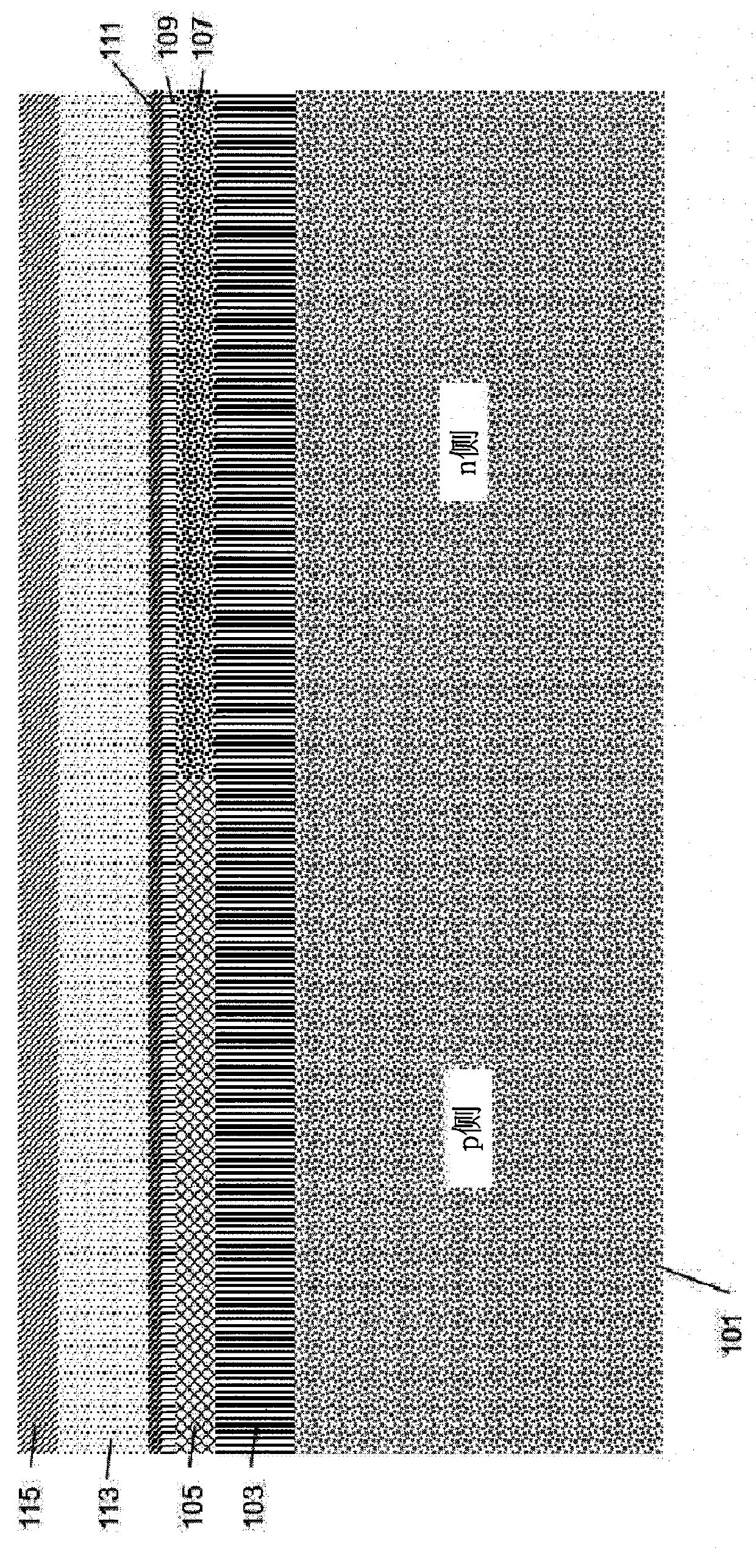
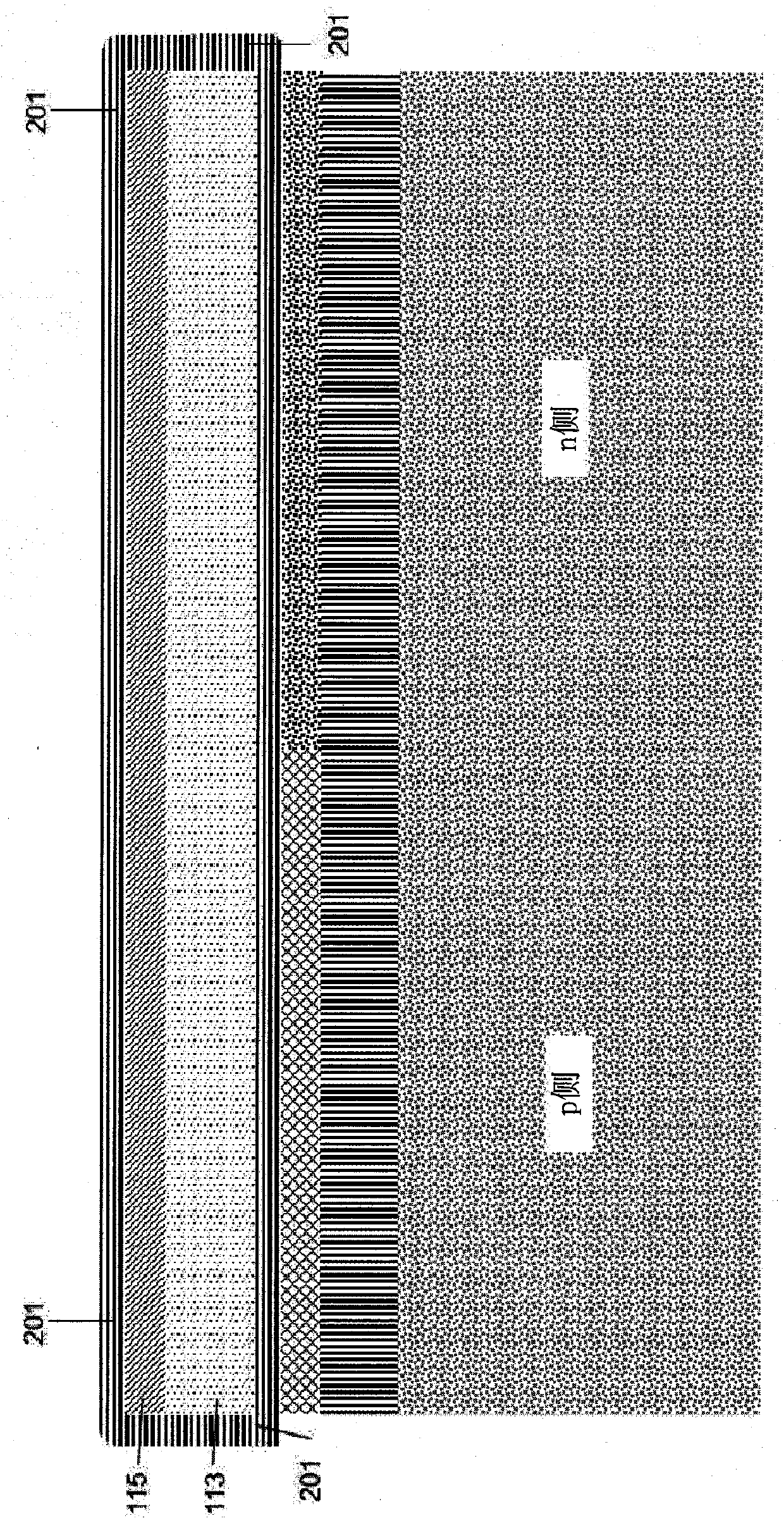
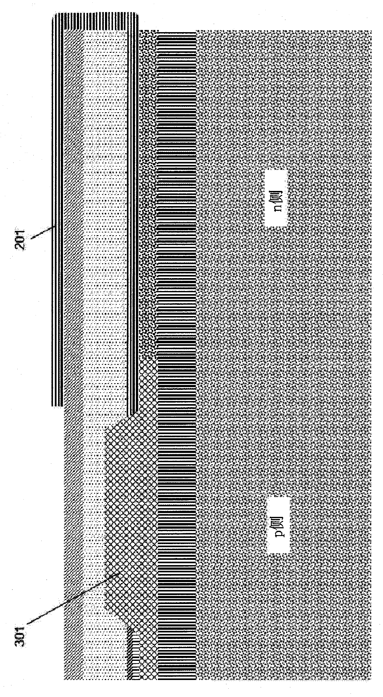
[0017] The present invention addresses and solves the current MOL and BEOL layer crowding problems in advanced cluster library configurations such as via contacts, without compromising the design rules of CB-PC contacts.
[0018] A method ac...
PUM
 Abstract
Description
Claims
Application Information
 - R&D
- Intellectual Property
- Life Sciences
- Materials
- Tech Scout
- Unparalleled Data Quality
- Higher Quality Content
- 60% Fewer Hallucinations
Browse by: Latest US Patents, China's latest patents, Technical Efficacy Thesaurus, Application Domain, Technology Topic, Popular Technical Reports.
© 2025 PatSnap. All rights reserved.Legal|Privacy policy|Modern Slavery Act Transparency Statement|Sitemap|About US| Contact US: help@patsnap.com