A method of embolization

A technology for a plug and a plug portion is applied in the field of a plug forming method and a semiconductor device having the plug, which can solve the problems of great influence on the device performance, unfavorable metal layer conduction, and difficulty in uniform entry of tungsten, etc., so as to increase the read/write speed. , lower temperature, the effect of uniform and dense inside

Active Publication Date: 2018-05-18
CHANGXIN MEMORY TECH INC
View PDF5 Cites 0 Cited by
  • Summary
  • Abstract
  • Description
  • Claims
  • Application Information

AI Technical Summary

Problems solved by technology

[0003] The quality of plug formation has a great influence on the performance of the device. If the quality of plug formation is poor, it will increase the interconnection resistance and affect the performance of the device.
However, as the process node continues to shrink, the aspect ratio of the hole opening used to form the plug also increases accordingly, so it is easy to make it difficult for the chemical vapor deposited tungsten to enter the bottom of the hole uniformly, and it is easy to form on the side wall surface of the hole opening. Build-up, causing the tungsten deposited into the hole to close prematurely at the opening before completely filling the hole, causing voids inside the formed plug, resulting in poor performance of the formed plug
Furthermore, when the excess tungsten metal is subsequently removed by chemical mechanical grinding or etching process, the cavities or gaps in the plug will be exposed, resulting in void defects in the formed plug, which will affect the reliability of the subsequent connection of the device
In the prior art, parameters such as lowering the temperature, adjusting the pressure, and air flow during the chemical vapor deposition process are often used to reduce the generation of voids or gaps, but the resistance of the tungsten plugs deposited under such an environment is too high, which is not conducive to the formation of the metal layer. conduction between

Method used


Image

  • A method of embolization
  • A method of embolization
  • A method of embolization

Examples


Embodiment

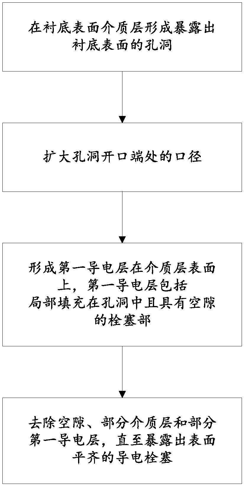
[0068] A method for forming a plug, comprising the steps of:

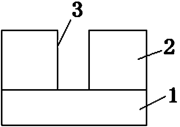
[0069] 1) a semiconductor substrate 1 is provided, a dielectric layer 2 is formed on the surface of the substrate 1 by a chemical vapor deposition process, and a hole 3 exposing the upper surface of the substrate 1 is formed on the dielectric layer 2 by an anisotropic dry etching process;

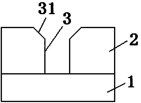
[0070] 2) using sputtering process or in-situ ashing process to expand the aperture at the opening end 31 of the hole 3, and relatively reduce the aspect ratio of the hole 3;

[0071] 3) Depositing Co, CoSi and Co into the interior of the hole 3 at the open end 31 of the hole 3 2 Combination materials of Si;

[0072] 4) An annealing process is performed after the deposition, and the composite material forms a layer of CoSi deposited on the bottom of the hole 3 through the reaction. 2 the second conductive layer 7;

[0073] 5) after forming the second conductive layer 7, a wet cleaning process is performed to remove the surfac...


PUM


Abstract

The invention relates to a plug formation method and a semiconductor device equipped with the plug. The plug formation method comprises the steps of providing a substrate, forming a dielectric layer on the surface of the substrate, and forming a hole in the dielectric layer; expanding the caliber in the opening end of the hole; forming a first conductive layer on the surface of the dielectric layer, wherein the first conductive layer comprises a plug part partially filled in the hole; and removing the gap, a part of the dielectric layer and a part of the first conductive layer to expose the conductive plug with the parallel and level surface. According to the semiconductor device, the dielectric layer is arranged on the surface of the substrate; the hole is formed in the dielectric layer; the hole is filled with the conductive plug; the surface of the conductive plug is parallel and level and exposed from the dielectric layer; and the conductive plug is a solid surface. The conductive plug formed by the method disclosed in the invention has the advantages of no gap, low resistance, high reliability and the like.

Description

technical field [0001] The present invention relates to the technical field of semiconductors, and in particular, to a method for forming a plug and a semiconductor device having the plug. Background technique [0002] Currently, in a semiconductor memory device, the electrical connection between the two metal layers is usually realized by forming a plug structure between the two metal layers. Because metal tungsten has good step coverage and gap filling properties, chemical vapor deposition of tungsten is often used to form plugs. [0003] The formation quality of the plug has a great influence on the performance of the device. If the formation quality of the plug is poor, the interconnect resistance will increase and the performance of the device will be affected. However, as the process node continues to shrink, the aspect ratio of the hole opening for forming the plug is also increased accordingly, so it is easy to make it difficult for the tungsten deposited by chemica...

Claims


Application Information

Patent Timeline
Patent Type & Authority Patents(China)
IPC IPC(8): H01L21/768
CPCH01L21/76816H01L21/76877H01L23/5283H01L2221/101H01L2221/1068
Inventor 不公告发明人
Owner CHANGXIN MEMORY TECH INC
Why Eureka
Try Eureka