

Laminated OLED display panel, manufacturing method thereof and display device
A technology for a display panel and a manufacturing method, which is applied in the manufacturing of semiconductor/solid-state devices, electrical components, and electrical solid-state devices, etc., can solve problems such as pixel crosstalk, and achieve the effects of increasing impedance, saving processing time, and improving pixel leakage.
- Summary
- Abstract
- Description
- Claims
- Application Information
AI Technical Summary
Problems solved by technology
Method used
Image

Examples
Embodiment Construction
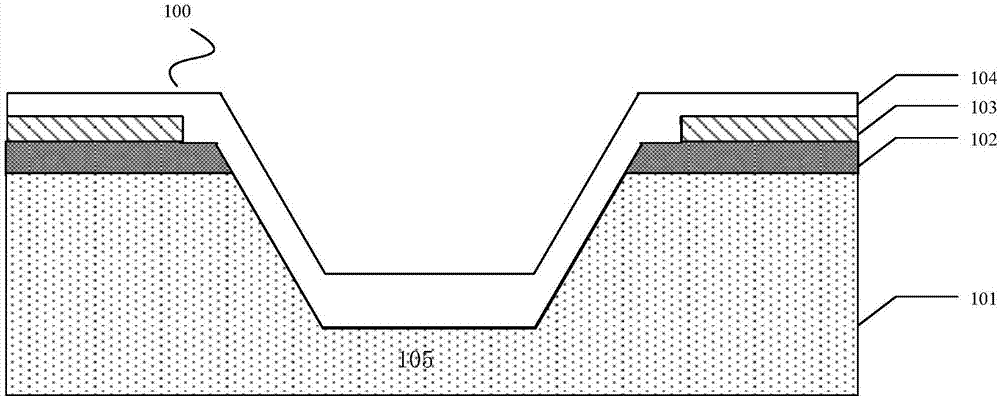
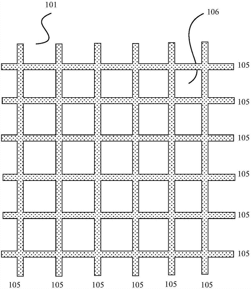
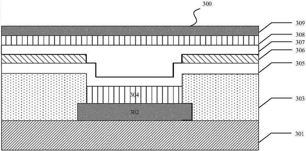
[0041] Example embodiments will now be described more fully with reference to the accompanying drawings. Example embodiments may, however, be embodied in many forms and should not be construed as limited to the examples set forth herein; rather, these embodiments are provided so that this disclosure will be thorough and complete and fully convey the concept of example embodiments to those skilled in the art. The described features, structures, or characteristics may be combined in any suitable manner in one or more embodiments. In the following description, numerous specific details are provided in order to give a thorough understanding of embodiments of the invention. However, those skilled in the art will appreciate that the technical solution of the present invention may be practiced without one or more of the specific details, or other methods, components, devices, steps, etc. may be adopted. In other instances, well-known technical solutions have not been shown or descr...
PUM
 Abstract
Description
Claims
Application Information