Pixel circuit, pixel structure and display panel

A technology of pixel circuit and display panel, which is applied in the field of pixel circuit, pixel structure and display panel, can solve the problem that the display panel is difficult to be compatible with the requirements of picture quality of human-computer interaction function and so on.

Inactive Publication Date: 2017-12-15
BOE TECH GRP CO LTD +1
View PDF9 Cites 12 Cited by
  • Summary
  • Abstract
  • Description
  • Claims
  • Application Information

AI Technical Summary

Problems solved by technology

[0005] The technical problem to be solved by the embodiments of the present invention is to provide a pixel circuit, a pixel structure and a display panel to solve the technical problem that the display panel in the prior art is difficult to be compatible with the realization of human-computer interaction functions and the requirements for picture quality

Method used


Image

  • Pixel circuit, pixel structure and display panel
  • Pixel circuit, pixel structure and display panel
  • Pixel circuit, pixel structure and display panel

Examples


no. 1 example

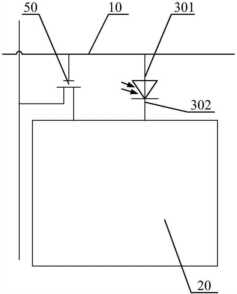
[0041] figure 2 It is a schematic diagram of the principle of the pixel circuit of the embodiment of the present invention. From figure 2 It can be seen from the figure that the pixel circuit in this embodiment of the present invention includes a first thin film transistor 50, a gate line 10 and a pixel electrode 20, and also includes a photosensitive unit, the first end 301 and the second end 302 of the photosensitive unit are connected to the gate line 10 and the second end 302 respectively. The pixel electrode 20 is connected, and the photosensitive unit is used to transmit the signal of the gate line 10 to the pixel electrode 20 when receiving a light signal. When the photosensitive unit receives the light signal, the first end 301 and the second end 302 are turned on, so as to transmit the signal of the gate line 10 to the pixel electrode 20 .

[0042] In the embodiment of the present invention, a method of realizing the human-computer interaction function of the disp...

no. 2 example

[0049] The main structure of the second embodiment of the present invention is the same as that of the above-mentioned first embodiment. In this embodiment, the structure of the photosensitive unit will be explained in detail.

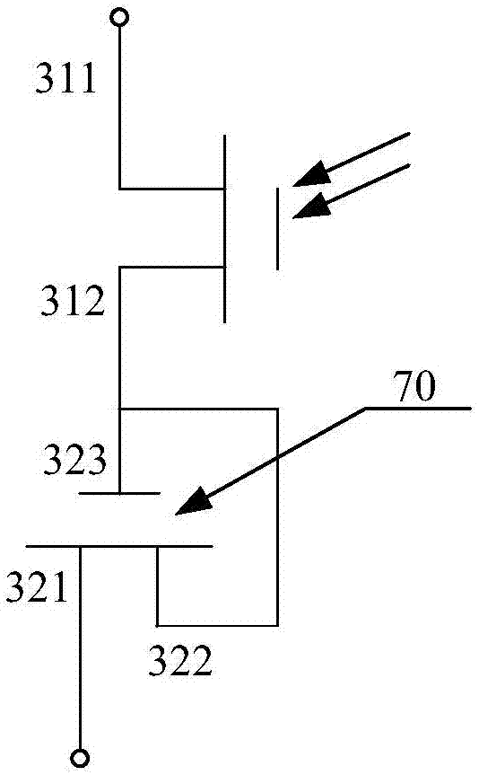
[0050] image 3 It is a schematic structural diagram of the photosensitive unit of the second embodiment of the present invention. The photosensitive unit in this embodiment includes a photosensitive device and a second thin film transistor 70, the first pole 311 of the photosensitive device is connected to the gate line, the second pole 312 of the photosensitive device is connected to the control electrode 323 of the second thin film transistor 70, and the second pole 311 of the photosensitive device is connected to the gate line. The first electrode 322 of the TFT 70 is connected to the control electrode 323 of the second TFT 70 , and the second electrode 321 of the second TFT 70 is connected to the pixel electrode.

[0051] The photosensitive devi...

no. 3 example

[0059] Figure 4 It is a schematic structural diagram of the photosensitive unit of the third embodiment of the present invention. Different from the second embodiment, the photosensitive unit in the embodiment of the present invention includes a photodiode, the anode 331 of the photodiode is connected to the gate line, and the cathode 332 of the photodiode is connected to the pixel electrode.

[0060] When the photodiode does not receive the light signal, the anode 331 and the cathode 332 are turned off, and the pixel electrode is normally controlled by the first thin film transistor; transmitted to the pixel electrode. The photosensitive diode is unidirectional, so it can prevent the pixel electrode from interfering with the signal of the gate line.

[0061] During the preparation process of the pixel circuit, preferably, the photosensitive structure of the photodiode and the active layer of the first thin film transistor are arranged in the same layer, and are formed by o...


PUM


Abstract

The embodiment of the invention provides a pixel circuit, a pixel structure and a display panel. The pixel circuit comprises a first thin film transistor, a grid, a pixel electrode and a light sensing unit. The first end and the second end of the light sensing unit are connected with the grid and the pixel electrode respectively. The light sensing unit is used for transmitting a signal of the grid to the pixel electrode when receiving a light signal. The embodiment of the invention further provides the pixel structure with the pixel circuit and the display panel. By arranging the light sensing unit, the light sensing unit transmits the signal of the grid to the pixel electrode when receiving the light signal, lights up corresponding pixels and displays a designated position for a user by presenting a partial bright spot, the man-machine interaction function is achieved, and the requirements of the display panel for the image quality are met.

Description

technical field [0001] The present application relates to but not limited to the field of display technology, especially a pixel circuit, a pixel structure and a display panel. Background technique [0002] Currently, there are various modes of operating the display, for example, mouse operation, remote control operation, and touch operation. With the development and upgrading of display technology, users have put forward more requirements for the functions and operation methods of the display, and human-computer interaction operation has become a development direction of remote control operation. [0003] Displays in the prior art, for example, Thin Film Transistor-Liquid Crystal Display (TFT-LCD for short) and Organic Light-Emitting Diode (OLED for short) are passive display structures. The following takes TFT-LCD as an example to illustrate. The light emitted by the backlight passes through the lower polarizer, modulated by liquid crystal (LC) and then detected by the up...

Claims


Application Information

Patent Timeline
Patent Type & Authority Applications(China)
IPC IPC(8): G02F1/1362G02F1/1368G02F1/1335G02F1/133
CPCG02F1/13306G02F1/133512G02F1/136286G02F1/1368H01L27/14643G02F1/13318G02F2201/123H01L27/124G02F2201/121
Inventor 刘德强王菲菲朱宁董霆孙志华高玉杰
Owner BOE TECH GRP CO LTD
Why Eureka
Try Eureka