CMOS device and fabrication method thereof

A manufacturing method and device technology, which is applied in semiconductor/solid-state device manufacturing, electrical components, transistors, etc., can solve problems such as the inability to realize multi-threshold regulation well, and achieve threshold adjustment with little influence, high control precision, and integrated The effect of simple process

Active Publication Date: 2017-12-15
INST OF MICROELECTRONICS CHINESE ACAD OF SCI +1
View PDF4 Cites 2 Cited by
  • Summary
  • Abstract
  • Description
  • Claims
  • Application Information

AI Technical Summary

Problems solved by technology

[0003] After entering the nanometer node, the adjustment of the threshold voltage of CMOS devices has always been an important and difficult point in the manufacture of semiconductor devices. At present, it is mainly adjusted by adjusting ion implantation, gate length, gate dielectric layer thickness and work function layer thickness. The threshold voltage of semiconductor devices, and with the further reduction in the size of semiconductor devices, especially when entering below the 10nm node, multiple threshold voltages need to be adjusted, but due to the space constraints and parasitic effects brought about by the size reduction, Higher requirements are put forward for the threshold adjustment of CMOS devices, and these traditional methods can no longer achieve multi-threshold adjustment well.

Method used


Image

  • CMOS device and fabrication method thereof
  • CMOS device and fabrication method thereof
  • CMOS device and fabrication method thereof

Examples


Embodiment Construction

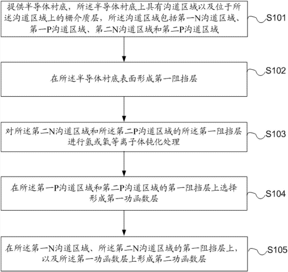
[0029] As mentioned in the background technology section, due to the space limitation and parasitic effects caused by size reduction in the prior art, higher requirements are put forward for the threshold adjustment of CMOS devices, and the traditional threshold adjustment method has not been well realized. Multi-threshold regulation.

[0030] Specifically, the method for adjusting the threshold of a CMOS device in the prior art is: first deposit a barrier layer on the metal gates of the NMOS region and the PMOS region, then adjust the thickness of the barrier layer, then deposit a PMOS work function layer (PMOS WFL), and then change The thickness of the PMOSWFL is used to adjust the PMOS threshold; the NMOS work function layer (NMOS WFL) is then deposited, and the NMOS WFL is combined with the change in the thickness of the previous barrier layer to jointly adjust the NMOS threshold. Since the NMOS threshold adjustment process in the existing method needs to be divided into t...


PUM


Abstract

The invention provides a CMOS device and a fabrication method thereof. The method comprises steps: a semiconductor substrate is provided; a first blocking layer is formed on the surface of the semiconductor substrate; hydrogen or oxygen plasma passivation processing is carried out on the first blocking layer on a second N channel area and a second P channel area; a first work function layer is formed on the first blocking layer on a first P channel area and the second P channel area; a second work function layer is formed on the first blocking layer on a first N channel area and the second N channel area and the first work function layer; and/or hydrogen or oxygen plasma passivation processing is carried out on the first blocking layer on the second N channel area and the first work function layer on the second P channel area. The method is high in threshold adjustment control precision, the process flexibility is high, and the method is simple and easy to operate and is more suitable for multi-threshold regulation on a small-size device.

Description

technical field [0001] The present invention relates to the technical field of semiconductor device manufacturing, and more specifically, to a CMOS (Complementary Metal Oxide Semiconductor, Complementary Metal Oxide Semiconductor) device and a manufacturing method thereof. Background technique [0002] As the integration level of integrated circuits continues to increase, the size of devices continues to decrease. It is difficult for traditional planar CMOS (Complementary Metal Oxide Semiconductor) devices to continue to reduce the key dimensions. Three-dimensional devices such as FINFET (Fin Field Effect Transistor) and Nanowire channel devices are gradually becoming the mainstream trend. [0003] After entering the nanometer node, the adjustment of the threshold voltage of CMOS devices has always been an important and difficult point in the manufacture of semiconductor devices. At present, it is mainly adjusted by adjusting ion implantation, gate length, gate dielectric la...

Claims


Application Information

Patent Timeline
Patent Type & Authority Applications(China)
IPC IPC(8): H01L21/8238H01L27/092
CPCH01L21/823807H01L27/092
Inventor 殷华湘姚佳欣赵超叶甜春
Owner INST OF MICROELECTRONICS CHINESE ACAD OF SCI
Why Eureka
Try Eureka