Laser annealing equipment and laser annealing method

A laser annealing and equipment technology, which is applied in the manufacture of electrical components, circuits, semiconductors/solid-state devices, etc., can solve the problems of non-transformation of the amorphous silicon layer, damage to the base, and influence on the transformation ratio of the polysilicon layer, and achieve the goal of increasing the transformation ratio Effect

Inactive Publication Date: 2017-12-19
BOE TECH GRP CO LTD +1
View PDF3 Cites 1 Cited by
  • Summary
  • Abstract
  • Description
  • Claims
  • Application Information

AI Technical Summary

Problems solved by technology

[0004] In the process of realizing the present invention, the inventors found that there are at least the following problems in related technologies: in order to avoid damage to the base platform by laser irradiation, the scanning area of ​​the linear spot on the amorphous silicon layer is difficult to completely cover the amorphous silicon layer. layer, which in turn causes part of the amorphous silicon layer not to be transformed into a polysilicon layer, which affects the transformation ratio of the polysilicon layer

Method used


Image

  • Laser annealing equipment and laser annealing method
  • Laser annealing equipment and laser annealing method
  • Laser annealing equipment and laser annealing method

Examples


Embodiment Construction

[0044] In order to make the object, technical solution and advantages of the present invention clearer, the implementation manner of the present invention will be further described in detail below in conjunction with the accompanying drawings.

[0045]The laser annealing equipment provided by various embodiments of the present invention can be used to carry out laser annealing to various materials, optionally, the laser annealing equipment provided by various embodiments of the present invention can be the excimer laser annealing that can emit excimer laser ( English: Excimer Laser Annealing; Abbreviation: ELA) equipment.

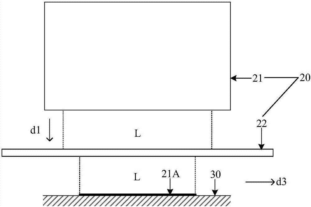
[0046] diagram 2-1 It is a structural schematic diagram of a laser annealing device shown in an embodiment of the present invention. The laser annealing equipment 20 may include:

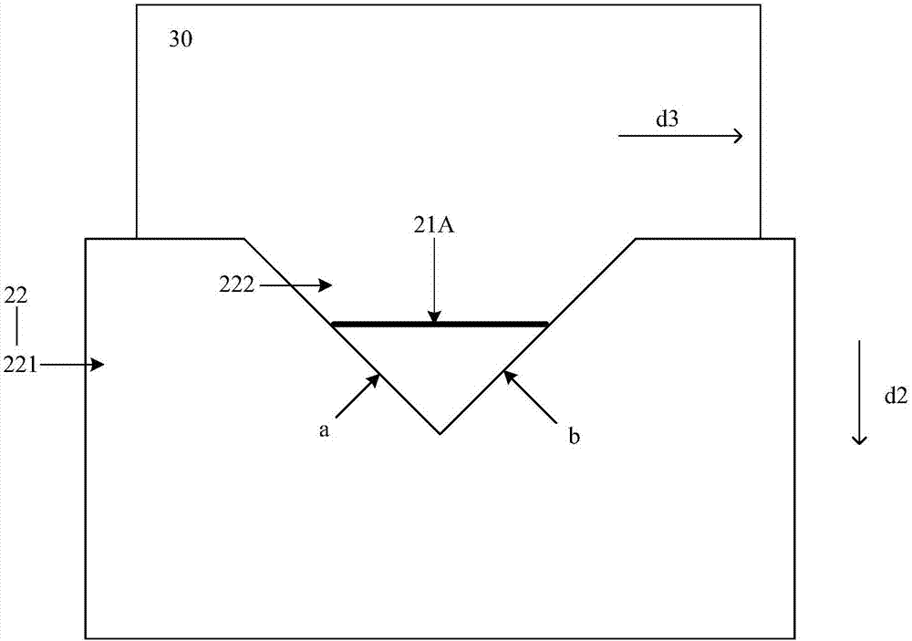
[0047] The linear laser 21 and the light cutter 22 arranged in the light emitting direction d1 of the linear laser 21 . The length direction of the linear spot 21A of the lin...


PUM


Abstract

The invention discloses laser annealing equipment and a laser annealing method and belongs to the technical field of display. The laser annealing equipment comprises a linear laser and a light cutter arranged in a light outlet direction of the linear laser, wherein the light cutter comprises a plate-shaped body; the plate-shaped body is provided with a hollow area limited by at least two edges; two edges of the hollow area are gradually close to each other along a default direction; and the length direction of a linear light spot of the linear laser on a default irradiation surface is not parallel to the default direction. When the light cutter and the linear laser relatively move along the default direction, the length of the light spot of the linear laser can be adjusted; and when an amorphous silicon layer is irradiated, the whole amorphous silicon layer can be transformed into a polysilicon layer through adjusting the length of the light spot, so that the problem that the transformation ratio of the polysilicon layer is affected due to the fact that one part of amorphous silicon layer is not transformed into the polysilicon layer in related technologies is solved, thereby achieving the effect of improving the transformation ratio of the polysilicon layer.

Description

technical field [0001] The invention relates to the field of display technology, in particular to a laser annealing device and a laser annealing method. Background technique [0002] Laser annealing (English: laser annealing) equipment usually includes a line laser (that is, a laser that emits a laser with a linear spot on the irradiation surface) and a light cutter (English: beam) for limiting the spot length of the line laser. cutter). Currently, laser annealing equipment is widely used in the process of forming polysilicon. [0003] In the related art, when polysilicon is formed, a rectangular amorphous silicon layer is formed in a predetermined area of ​​the base, and a light cutter is arranged between the amorphous silicon layer and the linear laser, and a strip-shaped hollow area is arranged on the light cutter. The length of the strip hollow area is shorter than the length of the linear spot of the linear laser. When the laser emitted by the line laser irradiates t...

Claims


Application Information

Patent Timeline
Patent Type & Authority Applications(China)
IPC IPC(8): H01L21/67H01L21/268
CPCH01L21/268H01L21/67115
Inventor 吕祖彬张宇谢璞谢银
Owner BOE TECH GRP CO LTD
Why Eureka
Try Eureka