Supercharge Your Innovation With Domain-Expert AI Agents!

Schottky base structure, schottky diode and manufacturing method therefor

A technology of Schottky diodes and anodes, applied in the direction of diodes, semiconductor/solid-state device manufacturing, electrical components, etc., can solve the problem of low reverse breakdown voltage, increased reverse voltage value, and increased reverse voltage value in the barrier region. Large and other problems, to achieve the effect of improving the reverse withstand voltage characteristics, increasing the reverse withstand voltage value, and increasing the reverse withstand voltage value

Active Publication Date: 2017-12-19
JIANGSU CORENERGY SEMICON CO LTD
View PDF5 Cites 0 Cited by
  • Summary
  • Abstract
  • Description
  • Claims
  • Application Information

AI Technical Summary

Problems solved by technology

[0003] However, due to the thinner depletion region of the Schottky diode, the reverse breakdown voltage is relatively low
In the prior art, when the Schottky diode is connected to the reverse voltage, an edge termination effect usually occurs at the edge of the connection between the anode metal and the N-type semiconductor, resulting in the accumulation of a large amount of positive charges at the connection between the N-type semiconductor and the edge of the anode metal , to generate an electric field in the same direction as the electric field generated by the reverse voltage, resulting in an increase in the reverse voltage value borne by the barrier region, and reverse breakdown of the Schottky diode
This is equivalent to indirectly reducing the reverse withstand voltage value of the Schottky diode, reducing the reliability of the Schottky diode, and affecting the normal operation of the circuit where the Schottky diode is located.
[0004] There are at least the following problems in the prior art: in the reverse connection state of the existing Schottky diodes, due to the edge termination effect between the anode metal and the N-type semiconductor, a large number of positive diodes are gathered at the junction of the N-type semiconductor and the edge of the anode metal. Charge, the accumulated positive charges will generate an electric field in the same direction as the electric field generated by the reverse voltage, resulting in an increase in the reverse voltage value borne by the barrier region, and reverse breakdown of the Schottky diode
This leads to an indirect reduction of the reverse withstand voltage value of the Schottky diode and reduces the reliability of the Schottky diode.

Method used


Image

  • Schottky base structure, schottky diode and manufacturing method therefor
  • Schottky base structure, schottky diode and manufacturing method therefor
  • Schottky base structure, schottky diode and manufacturing method therefor

Examples


Embodiment Construction

[0035] Embodiments of the present application provide a Schottky structure, a Schottky diode and a manufacturing method.

[0036] In order to enable those skilled in the art to better understand the technical solutions in the present application, the technical solutions in the embodiments of the present application will be clearly and completely described below in conjunction with the drawings in the embodiments of the present application. Obviously, the described The embodiments are only some of the embodiments of the present application, but not all of them. Based on the embodiments in this application, all other embodiments obtained by persons of ordinary skill in the art without creative efforts shall fall within the scope of protection of this application.

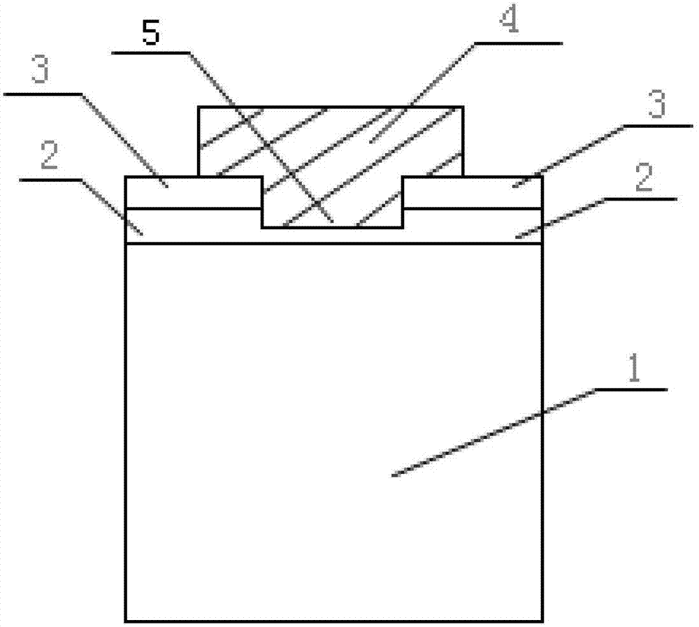
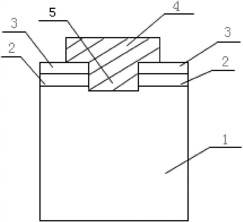
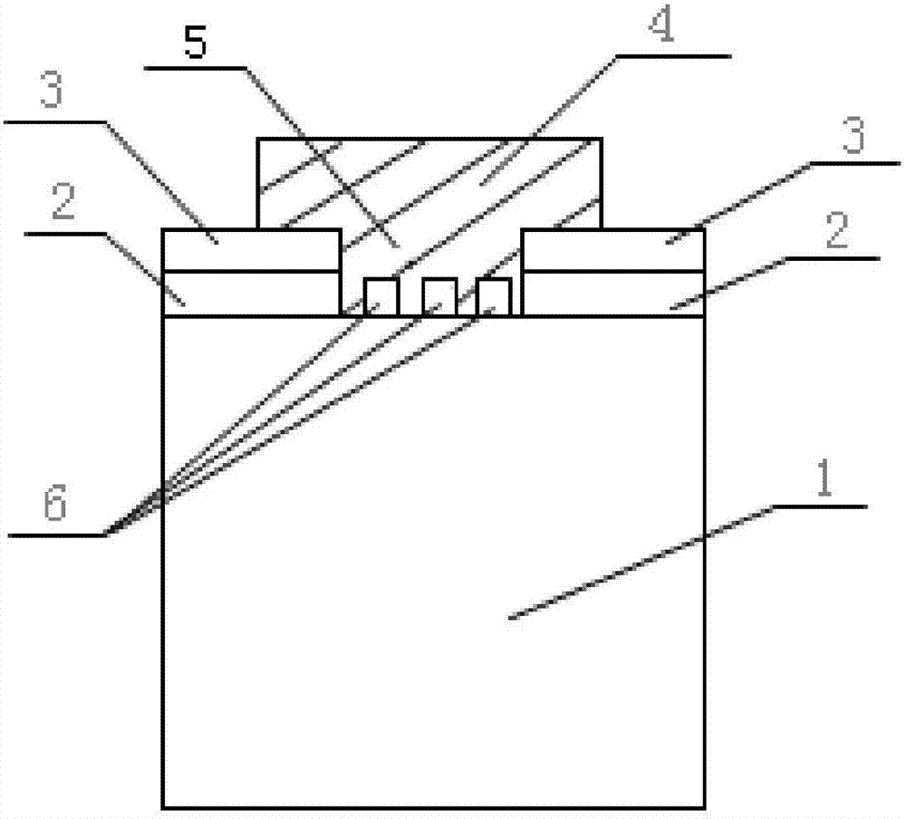
[0037] figure 1 is a structural schematic diagram of a Schottky structure described in this application. Although the present application provides method operation steps or structures as shown in the following embod...


PUM


Abstract

The invention provides a schottky base structure. The schottky base structure comprises an N type semiconductor layer, a first P type semiconductor layer which covers the N type semiconductor layer, and a first N type semiconductor layer or a semi-insulating type semiconductor layer which covers the first P type semiconductor layer. By virtue of the schottky base structure provided by the embodiment, the reverse voltage withstand value of the diode can be improved effectively, and reliability of the diode is effectively improved.

Description

technical field [0001] The present application relates to the technical field of semiconductor devices, in particular to a Schottky structure, a Schottky diode and a manufacturing method. Background technique [0002] Schottky diodes are diodes that use metal and N-type semiconductor contacts to form a barrier at the interface. Since the Schottky diode does not have the process of accumulation and dissipation of minority carriers near the PN junction, the capacitive effect is very small and the working speed is very fast, which is especially suitable for high frequency or switching state applications. [0003] However, due to the thinner depletion region of the Schottky diode, the reverse breakdown voltage is lower. In the prior art, when the Schottky diode is connected to the reverse voltage, an edge termination effect usually occurs at the edge of the connection between the anode metal and the N-type semiconductor, resulting in the accumulation of a large amount of posi...

Claims


Application Information

Patent Timeline
Patent Type & Authority Applications(China)
IPC IPC(8): H01L29/872H01L29/06H01L21/329
CPCH01L29/0619H01L29/66143H01L29/872H01L29/2003H01L29/0623H01L29/0611H01L29/66212H01L27/0928
Inventor 朱廷刚张葶葶李亦衡王东盛夏远洋
Owner JIANGSU CORENERGY SEMICON CO LTD
Features
  • R&D
  • Intellectual Property
  • Life Sciences
  • Materials
  • Tech Scout
  • Unparalleled Data Quality
  • Higher Quality Content
  • 60% Fewer Hallucinations
Learn More