OLED driving film transistor parameter obtaining method

A technology for obtaining thin film transistors and parameters, applied in instruments, static indicators, etc., can solve problems such as parameter deviation of driving thin film transistors, and achieve the effect of improving compensation uniformity

Active Publication Date: 2017-12-22
SHENZHEN CHINA STAR OPTOELECTRONICS SEMICON DISPLAY TECH CO LTD
View PDF6 Cites 13 Cited by
  • Summary
  • Abstract
  • Description
  • Claims
  • Application Information

AI Technical Summary

Problems solved by technology

It is generally considered that the gate-source voltage difference of the second thin film transistor T20 corresponding to the driving current is the difference between the preset gate voltage and the reference voltage Vref, but in fact, when the switch S10 is closed, due to the equivalent resistance of the wire 300 and The presence of the drain-source voltage across the third thin film transistor T30 makes the source voltage of the second thin film transistor T20 greater than the reference voltage Vref, that is, the gate-source voltage difference of the second thin film transistor T20 is not equal to the preset gate voltage The difference from the reference voltage Vref, so the parameters obtained to drive the thin film transistor will have a large deviation

Method used


Image

  • OLED driving film transistor parameter obtaining method
  • OLED driving film transistor parameter obtaining method
  • OLED driving film transistor parameter obtaining method

Examples


Embodiment Construction

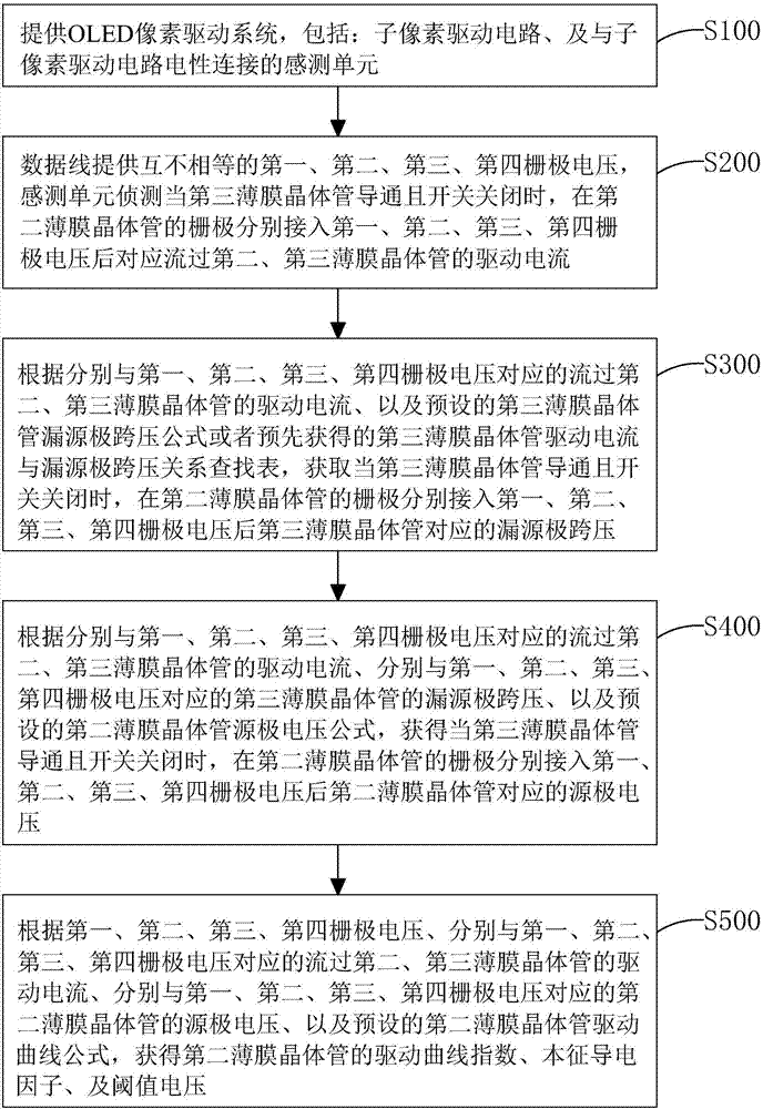
[0042] In order to further illustrate the technical means adopted by the present invention and its effects, the following describes in detail in conjunction with preferred embodiments of the present invention and accompanying drawings.

[0043] see figure 2 , the present invention provides a method for obtaining parameters of an OLED-driven thin film transistor, comprising the following steps:

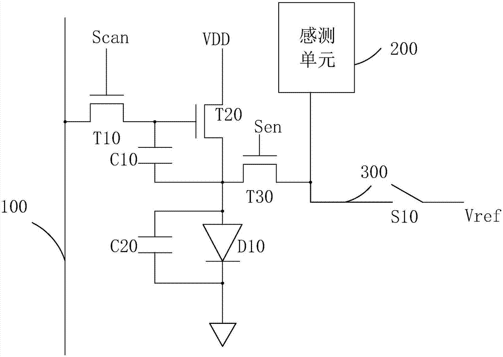
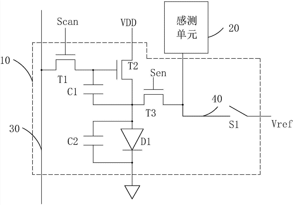
[0044] Step S100, please refer to image 3 , providing an OLED pixel driving system, including: a sub-pixel driving circuit 10, and a sensing unit 20 electrically connected to the sub-pixel driving circuit 10; the sub-pixel driving circuit 10 includes: a first thin film transistor T1, a second thin film transistor T2, the third thin film transistor T3, the first capacitor C1, the second capacitor C2, the organic light emitting diode D1, and the switch S1; the gate of the first thin film transistor T1 is connected to the scanning signal Scan, and the source is electrically connected t...


PUM


Abstract

The invention provides an OLED driving film transistor parameter obtaining method. The OLED driving film transistor parameter obtaining method comprises steps of using a data line to provide different first gate voltage, second gate voltage, third gate voltage and fourth gate voltage, using a sensing unit at a gate of a second film transistor to write the first gate voltage, the second gate voltage, the third gate voltage and the fourth gate voltage, wherein the source electrode of the second film transistor detects driving current flowing through a second film transistor and a third film transistor when a conducted third film transistor, a lead and a switched-off switch are connected to reference voltage, calculating a drain source electrode step voltage of a third film transistor according to current flowing through the second film transistor and the third film transistor and obtaining source electrode voltage of a more accurate second film transistor which corresponds to the first gate voltage, the second gate voltage, the third gate voltage and the fourth gate voltage so as to obtain accurate parameters of the driving film transistor. As a result, compensation is performed on an OLED panel according to the parameters of the driving film transistor in order to improve image compensation uniformity.

Description

technical field [0001] The invention relates to the field of display technology, in particular to a parameter acquisition method for OLED driving thin film transistors. Background technique [0002] Organic light emitting diode (Organic Light Emitting Display, OLED) display device has self-illumination, low driving voltage, high luminous efficiency, short response time, high definition and contrast, nearly 180° viewing angle, wide operating temperature range, and can realize flexible display and With many advantages such as large-area full-color display, it is recognized by the industry as a display device with the most potential for development. [0003] OLED display devices can be divided into passive matrix OLED (Passive Matrix OLED, PMOLED) and active matrix OLED (Active Matrix OLED, AMOLED) two categories according to the driving method, namely direct addressing and thin film transistor (Thin Film Transistor, TFT) matrix addressing two types. Among them, AMOLED has pi...

Claims


Application Information

Patent Timeline
Patent Type & Authority Applications(China)
IPC IPC(8): G09G3/3233
Inventor 梁鹏飞曾玉超
Owner SHENZHEN CHINA STAR OPTOELECTRONICS SEMICON DISPLAY TECH CO LTD
Why Eureka
Try Eureka