Solder-resistant processing method of PCB and PCB

A processing method and PCB board technology, applied in the secondary processing of printed circuits, electrical components, printed circuit manufacturing, etc., can solve problems such as thin ink, and achieve the effect of solving the problem of thin ink on the edge of the line

Active Publication Date: 2017-12-22
SHENZHEN KINWONG ELECTRONICS
View PDF7 Cites 8 Cited by
  • Summary
  • Abstract
  • Description
  • Claims
  • Application Information

AI Technical Summary

Problems solved by technology

[0005] In view of the above-mentioned deficiencies in the prior art, the object of the present invention is to provide a PCB solder mask treatment method and a PCB board, aiming to solve the problem of inkjet printing ink in the circuit area in the existing solder mask digital inkjet printing technology. thin question

Method used


Image

  • Solder-resistant processing method of PCB and PCB
  • Solder-resistant processing method of PCB and PCB
  • Solder-resistant processing method of PCB and PCB

Examples


Embodiment 1

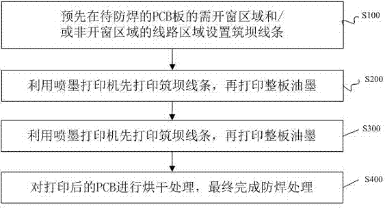
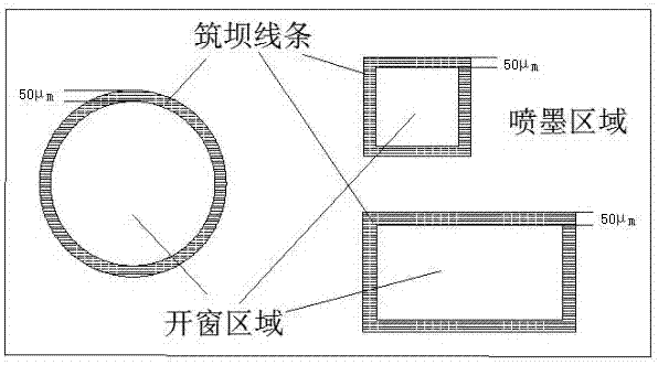
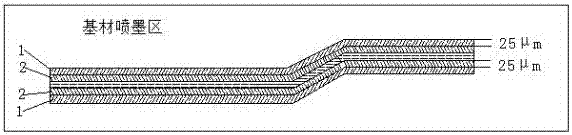
[0060] Step 1: CAM design: set damming lines with a line width of 50 μm in the area where the window needs to be opened and the line area in the non-opening area. The base material area where the window area intersects; the dam line in the line area located in the non-window area partially covers the copper surface of the line, and partly covers the base material area of ​​the window area, and the line width of both parts is 25um;

[0061] Step 2: Pre-treatment of inkjet printing: pickling, super-roughening, and anti-rust treatment on the copper surface of the PCB board before solder masking. The amount is controlled at 0.8μm, and the copper surface antirust treatment time is 40s;

[0062] Step 3: Anti-seepage oil treatment before inkjet printing: soak the PCB board after inkjet printing pretreatment in the ink anti-seepage liquid for 40s, then put it into a horizontal cleaning line with a water washing spray pressure of 6psi for 60s, and finally Then dry the cleaned PCB boar...


PUM

PropertyMeasurementUnit
Line widthaaaaaaaaaa
Wavelengthaaaaaaaaaa

Abstract

The invention discloses a solder-resistant processing method of a PCB and a PCB. The method comprises: damming lines are arranged in line areas of an area needing windowing and a non-windowing area at a PCB on which solder-resistant processing is going to be carried in advance; and the damming lines are printed by using an ink-jet printer and then ink of the whole board is printed. According to the invention, the damming lines are arranged in the area needing windowing, the damming lines are printed by using the ink-jet printer, and the ink is printed on the board, so that a problem of the thin ink at the edge of the solder-resistant digital ink-jet printer line is solved. Meanwhile, super-roughening processing is carried out before printing, so that a problem of ink leakage during the jet printing process of the solder-resistant digital ink-jet printer technology as well as a problem of weak ink adhesive force after solder-resistant digital ink-jet printing is solved.

Description

technical field [0001] The invention relates to the field of PCB boards, in particular to a PCB solder-proof treatment method and a PCB board. Background technique [0002] The traditional PCB solder mask screen printing manufacturing process needs five steps including pretreatment, screen printing ink, pre-baking, exposure and development, while the solder mask digital inkjet printing technology only needs to go through three steps: circuit board surface treatment, solder mask printing and post-baking. One step completes the entire process. Compared with the traditional solder mask screen printing process, solder mask digital inkjet printing technology eliminates the production process of photographic film, screen plate production process and screen printing equipment, avoids the process and equipment of ink exposure and development, and simplifies PCB Improve the production process and shorten the production cycle, reduce production equipment and save costs, thereby achie...

Claims


Application Information

Patent Timeline
IPC IPC(8): H05K3/28
CPCH05K3/282
Inventor 付凤奇王俊陆玉婷
Owner SHENZHEN KINWONG ELECTRONICS
Why Eureka
Try Eureka