Fin field effect transistor and method of forming the same

A fin field effect and transistor technology, which is applied in semiconductor devices, semiconductor/solid state device manufacturing, electrical components, etc., can solve the problems of poor performance of fin field effect transistors, and improve stress, reduce collapse, and performance Improved effect

Active Publication Date: 2021-05-04
SEMICON MFG INT (SHANGHAI) CORP +1
View PDF4 Cites 0 Cited by
  • Summary
  • Abstract
  • Description
  • Claims
  • Application Information

AI Technical Summary

Problems solved by technology

[0004] However, the FinFETs formed by the prior art have poor performance

Method used


Image

  • Fin field effect transistor and method of forming the same
  • Fin field effect transistor and method of forming the same
  • Fin field effect transistor and method of forming the same

Examples


Embodiment Construction

[0029] As mentioned in the background, the performance of FinFETs formed in the prior art is poor.

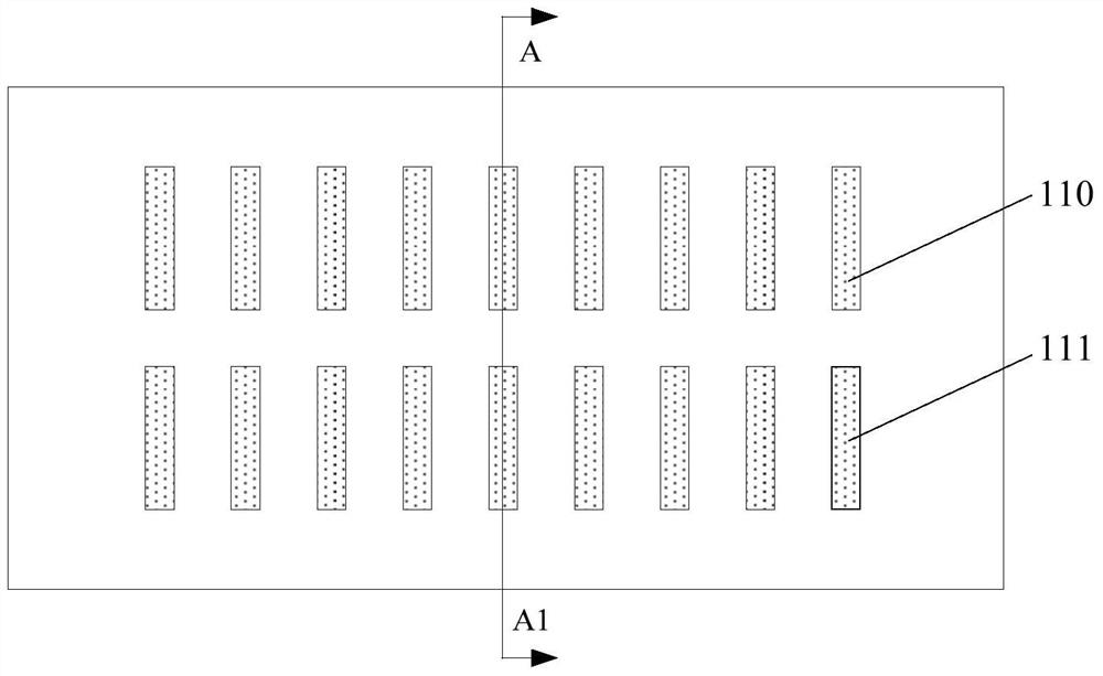
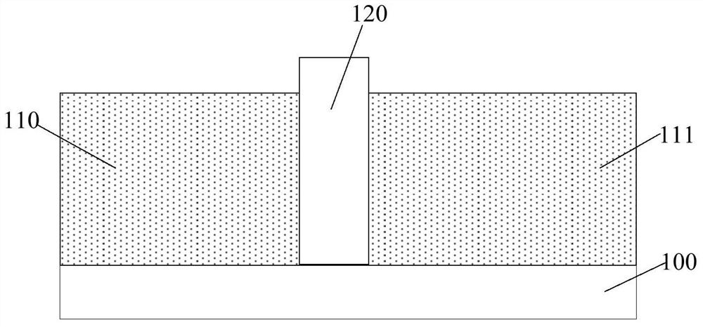
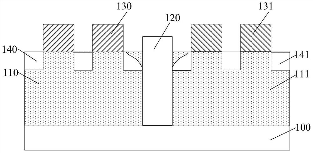
[0030] Figure 1 to Figure 3 It is a structural schematic diagram of the formation process of a fin field effect transistor.

[0031] combined reference figure 1 and figure 2 , figure 2 for along figure 1 The schematic diagram obtained by cutting line A-A1 in the middle provides a semiconductor substrate 100 with initial fins on the semiconductor substrate 100; the initial fins are cut along the normal direction of the surface of the semiconductor substrate 100, and the initial fins are divided into first fins 110 and second fins 111; an isolation structure and an isolation layer 120 are formed on the semiconductor substrate 100, the isolation structure is located between adjacent first fins 110 and between adjacent second fins 111, and isolating The top surface of the structure is lower than the top surfaces of the first fin portion 110 and the second fin portion 111, ...


PUM


Abstract

A Fin Field Effect Transistor and a method for forming the same, wherein the method includes: providing a semiconductor substrate having a first initial fin; forming a first groove in the first initial fin; The first groove penetrates the first initial fin along the direction perpendicular to the extension of the first initial fin; an epitaxial layer is formed on the sidewall of the first initial fin exposed in the first groove; after the epitaxial layer is formed, the The first groove is filled with an isolation layer; after the isolation layer is formed, a gate structure across the first initial fin is formed; source and drain doped regions are formed in the first initial fin on both sides of the gate structure. The method improves the performance of FinFETs.

Description

technical field [0001] The invention relates to the field of semiconductor manufacturing, in particular to a fin field effect transistor and a forming method thereof. Background technique [0002] MOS transistors are one of the most important components in modern integrated circuits. The basic structure of a MOS transistor includes: a semiconductor substrate; a gate structure located on the surface of the semiconductor substrate, a source region located in the semiconductor substrate on one side of the gate structure, and a drain region located in the semiconductor substrate on the other side of the gate structure. The working principle of the MOS transistor is: by applying a voltage to the gate structure, the current through the channel at the bottom of the gate structure is adjusted to generate a switching signal. [0003] With the development of semiconductor technology, the ability of the traditional planar MOS transistor to control the channel current becomes weaker, r...

Claims


Application Information

Patent Timeline
Patent Type & Authority Patents(China)
IPC IPC(8): H01L21/336H01L29/08H01L29/10H01L29/78
CPCH01L29/0847H01L29/1033H01L29/66795H01L29/7848H01L29/785
Inventor 张海洋肖芳元
Owner SEMICON MFG INT (SHANGHAI) CORP
Why Eureka
Try Eureka