Fabrication method of semiconductor device
A manufacturing method and semiconductor technology, which are applied in semiconductor/solid-state device manufacturing, electrical components, circuits, etc., can solve the problems of uneven device yield of crystal edge film layers, and achieve the effect of avoiding device defects and uniform film layers.
- Summary
- Abstract
- Description
- Claims
- Application Information
AI Technical Summary
Problems solved by technology
Method used
Image

Examples
Embodiment 1
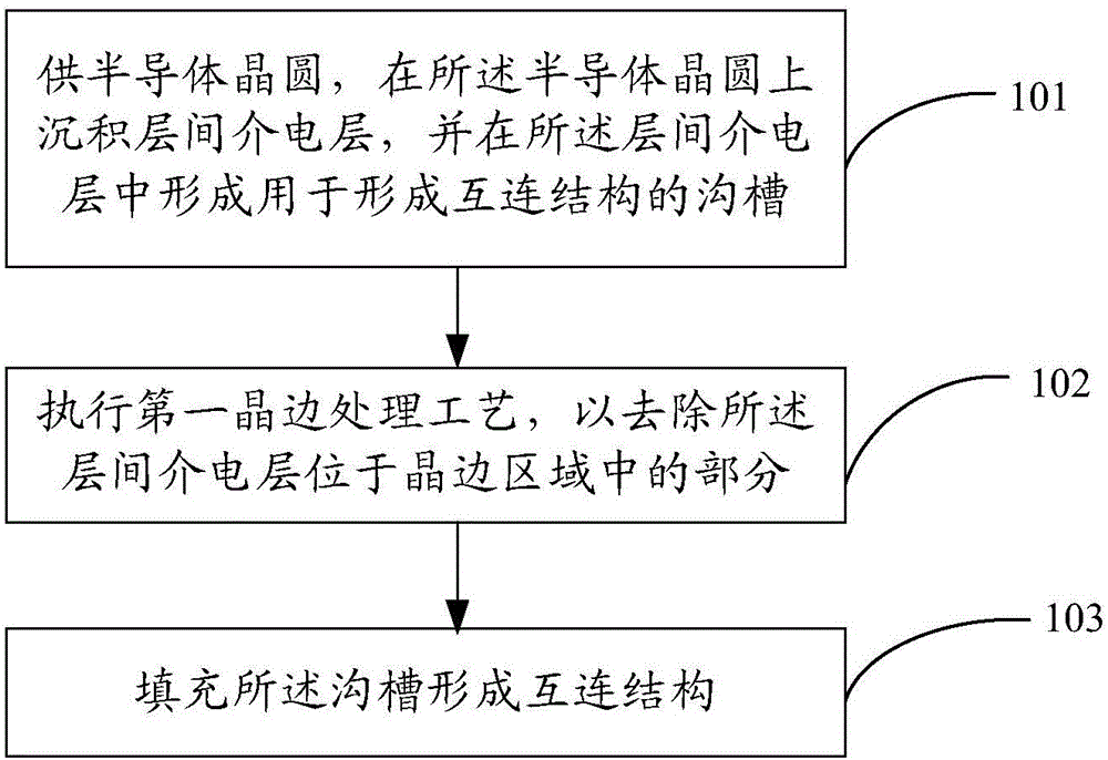
[0037] The following will refer to figure 1 A method for fabricating a semiconductor device according to an embodiment of the present invention will be described in detail.
[0038]As mentioned above, when forming the interconnection structure, due to the unevenness of the film layer at the grain edge, there are defects in the device. One embodiment of the present invention proposes a method for manufacturing a semiconductor device to overcome this problem, such as figure 1 As shown, the preparation method includes the following steps:
[0039] Step 101 , providing a semiconductor wafer, depositing an interlayer dielectric layer on the semiconductor wafer, and forming trenches for forming an interconnection structure in the interlayer dielectric layer.
[0040] Wherein, the semiconductor wafer can be at least one of the materials mentioned below: Si, Ge, SiGe, SiC, SiGeC, InAs, GaAs, InP or other III / V compound semiconductors, and multilayers composed of these semiconductors ...
Embodiment 2
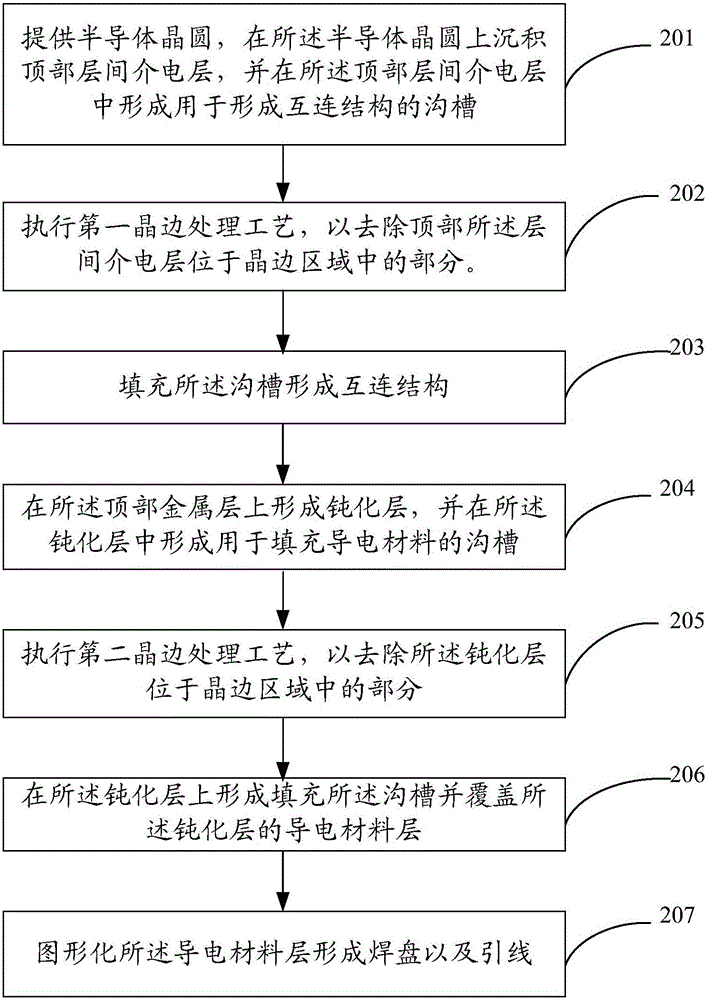
[0055] The following will refer to figure 2 A method for fabricating a semiconductor device according to another embodiment of the present invention is described in detail.
[0056] As mentioned above, when forming pads and leads, due to the unevenness of the film layer at the crystal edge, the device has defects such as aluminum out-of-focus and bridging. One embodiment of the present invention proposes a semiconductor device manufacturing method to overcome Such problems as figure 2 As shown, the preparation method includes the following steps:
[0057] Step 201 , providing a semiconductor wafer, depositing a top interlayer dielectric layer on the semiconductor wafer, and forming trenches for forming interconnection structures in the top interlayer dielectric layer.
[0058] Wherein, the semiconductor wafer can be at least one of the materials mentioned below: Si, Ge, SiGe, SiC, SiGeC, InAs, GaAs, InP or other III / V compound semiconductors, and multilayers composed of th...
Embodiment 3
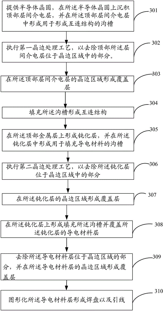
[0083] The following will refer to image 3 A method for fabricating a semiconductor device according to another embodiment of the present invention is described in detail.
[0084] As mentioned above, when forming pads and leads, due to the uneven film layer at the crystal edge, the device has defects such as aluminum defocusing and bridging. The semiconductor device proposed in an embodiment of the present invention overcomes this problem. Such as image 3 As shown, the preparation method includes the following steps:
[0085] Step 301 , providing a semiconductor wafer, depositing a top interlayer dielectric layer on the semiconductor wafer, and forming trenches for forming interconnection structures in the top interlayer dielectric layer.
[0086] Wherein, the semiconductor wafer can be at least one of the materials mentioned below: Si, Ge, SiGe, SiC, SiGeC, InAs, GaAs, InP or other III / V compound semiconductors, and multilayers composed of these semiconductors The struc...
PUM
 Abstract
Description
Claims
Application Information
 - R&D
- Intellectual Property
- Life Sciences
- Materials
- Tech Scout
- Unparalleled Data Quality
- Higher Quality Content
- 60% Fewer Hallucinations
Browse by: Latest US Patents, China's latest patents, Technical Efficacy Thesaurus, Application Domain, Technology Topic, Popular Technical Reports.
© 2025 PatSnap. All rights reserved.Legal|Privacy policy|Modern Slavery Act Transparency Statement|Sitemap|About US| Contact US: help@patsnap.com