Inductance adjustable device, electronic equipment and inductance adjustable method

A technology of electronic equipment and inductance, applied in the field of communication, can solve the problems of changing the impedance matching network, unable to add electronic equipment, and large space volume

Active Publication Date: 2021-03-16
BEIJING XIAOMI MOBILE SOFTWARE CO LTD
View PDF9 Cites 0 Cited by
  • Summary
  • Abstract
  • Description
  • Claims
  • Application Information

AI Technical Summary

Problems solved by technology

[0004] However, the space occupied by variable inductance devices on the market is relatively large, and technicians cannot add them to smaller electronic devices, resulting in the inability of electronic devices to change the impedance matching by changing the inductance value of the inductor in the impedance matching network. network impedance

Method used


Image

  • Inductance adjustable device, electronic equipment and inductance adjustable method
  • Inductance adjustable device, electronic equipment and inductance adjustable method
  • Inductance adjustable device, electronic equipment and inductance adjustable method

Examples


Embodiment Construction

[0033] Reference will now be made in detail to the exemplary embodiments, examples of which are illustrated in the accompanying drawings. When the following description refers to the accompanying drawings, the same numerals in different drawings refer to the same or similar elements unless otherwise indicated. The implementations described in the following exemplary examples do not represent all implementations consistent with the present disclosure. Rather, they are merely examples of apparatuses and methods consistent with aspects of the present disclosure as recited in the appended claims.

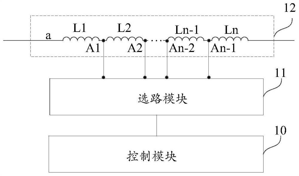
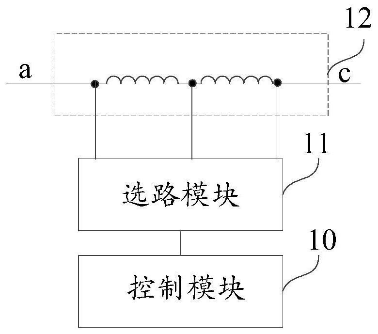
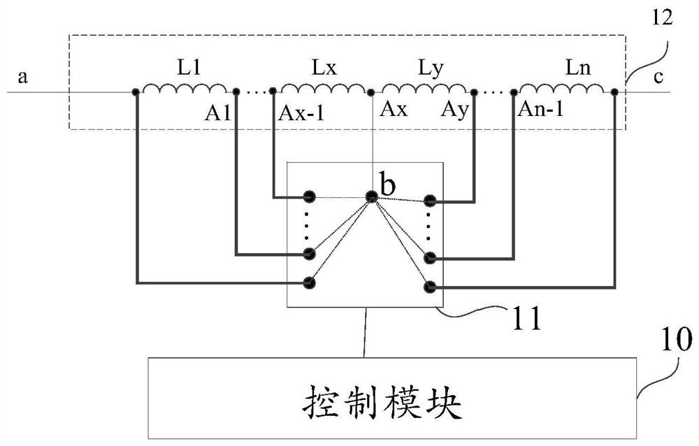
[0034] figure 1 is a schematic structural diagram of an adjustable inductance device according to an exemplary embodiment, as shown in figure 1 As shown, the adjustable inductance device includes a control module 10 , a routing module 11 and an inductance component 12 .

[0035] Wherein, the inductance component 12 includes n inductive circuits connected in series, where n≧2 and n is...


PUM


Abstract

The disclosure relates to an inductance adjustable device, an electronic device, and an inductance adjustable method, and belongs to the technical field of communication. The inductance adjustable device comprises a control module, a routing module and an inductor component. The inductor component comprises a plurality of inductive circuits connected in series. The control module is connected with the signal end of the routing module. Junctions between every two adjacent inductive circuits in the inductor component correspond to binding posts in the routing module one to one and are connected with respective corresponding binding posts. The control module adjusts the inductance value of the inductor component through the routing module. When at least two binding posts communicate with each other, at least one inductive circuit in the inductor component can be short-circuited to change the inductance value of the inductance adjustable device. The constituent parts of the inductance adjustable device can be designed in the electronic device because of occupying little space. The inductance adjustable device solves a problem that an electronic device in the prior art cannot change the inductance value of an inductor in an impedance matching network, and achieves an effect that the electronic device can adjust the inductance value in the impedance matching network.

Description

technical field [0001] The present disclosure relates to the technical field of communication, and in particular to an adjustable inductance device, electronic equipment and an adjustable inductance method. Background technique [0002] In current electronic equipment, an impedance matching network is connected between a radio frequency signal transmitter and an antenna. The sum of the impedance of the impedance matching network and the impedance of the antenna is equal to the impedance of the transmitter, and when the phase of the sum is the same as the phase of the impedance of the transmitter, the power of the radio frequency signal transmitted by the antenna can reach the highest. [0003] Since the impedance of the antenna will be affected by the power of the radio frequency signal it transmits, in order to ensure that the antenna can transmit the radio frequency signal at the maximum power at any frequency, electronic equipment usually needs to adjust the impedance mat...

Claims


Application Information

Patent Timeline
Patent Type & Authority Patents(China)
IPC IPC(8): H01Q23/00H01F21/12
CPCH01F21/12H01Q23/00
Inventor 刘文冬
Owner BEIJING XIAOMI MOBILE SOFTWARE CO LTD
Why Eureka
Try Eureka