Optical control integrated on-chip inductor

A technology of inductance and chip formation, applied in the direction of inductors, variable inductors, circuits, etc., can solve problems such as high noise level, poor circuit frequency stability, and reduced inductance quality factor Q

Pending Publication Date: 2019-05-21
CHINA JILIANG UNIV
View PDF0 Cites 0 Cited by
  • Summary
  • Abstract
  • Description
  • Claims
  • Application Information

AI Technical Summary

Problems solved by technology

However, the on-chip inductor is a fixed coil, and the shape, size, wire diameter, and number of turns of the coil have been determined. Under the condition of a certain frequency, the inductance value of the on-chip inductor can only be a certain value. cannot change
The inductor is affected by many parasitic effects such as the ohmic loss of the metal ...

Method used


Image

  • Optical control integrated on-chip inductor
  • Optical control integrated on-chip inductor

Examples


Embodiment Construction

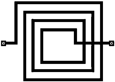
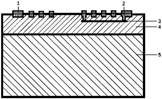
[0012] The manufacturing steps of the light-controlled integrated on-chip inductor are as follows.

[0013] A silicon wafer is selected, and a silicon dioxide layer is formed on the silicon wafer through a thermal oxidation process.

[0014] The bottom electrode of the inductor coil is made of copper, which is formed on the silicon dioxide layer by electroplating.

[0015] To isolate the bottom and top electrodes, an additional layer of silicon dioxide is deposited on the bottom electrode using plasma-enhanced chemical vapor deposition (PECVD).

[0016] The production of the inductance coil adopts the damascene process, and the dielectric layer is etched by the reactive ion process to form metal wiring grooves.

[0017] Then, a layer of metal copper that completely fills the groove and covers the entire silicon wafer is electroplated by an electroplating process, and a layer of optomagnetic material is formed on the surface of the copper by deposition.

[0018] Finally, chem...


PUM


Abstract

The invention provides an optical control integrated on-chip inductor, belonging to the technical field of microelectronic devices. An optical control inductor structure comprises a photomagnetic material, a metal wire, a silica isolation layer and a silicon substrate, wherein a photomagnetic material coil layer represents a main body of an optical control on-chip inductor and is arranged on the substrate, the photomagnetic material senses lighting change, results in change of overall magnetic conductivity of the coil through change of the magnetic conductivity, so as to change inductance. A silica insulating layer is added between the inductor coil and the substrate, and is used for isolating eddy loss of the substrate, further, the metal wire is made of a highly conductive material, so that ohmic loss of the metal is reduced, quality factor of the inductor is improved greatly, and overall performance of the circuit is improved.

Description

technical field [0001] This patent belongs to the technical field of microelectronic devices, and relates to an optically controlled integrated on-chip inductor. Background technique [0002] On-chip inductors are the basic passive components of radio frequency integrated circuits, and their shapes are as figure 1 As shown, it realizes the conversion and storage of electric energy to magnetic energy, and is widely used in various RF front-end modules such as low-noise amplifiers, voltage-controlled oscillators, mixers, and filters, forming the basis of wireless communication. However, the on-chip inductor is a fixed coil, and the shape, size, wire diameter, and number of turns of the coil have been determined. Under the condition of a certain frequency, the inductance value of the on-chip inductor can only be a certain value. Can't change. The inductor is affected by many parasitic effects such as the ohmic loss of the metal itself, the eddy current loss of the semiconduct...

Claims


Application Information

Patent Timeline
IPC IPC(8): H01F27/28H01F27/32H01F27/34H01F29/00
Inventor 唐莹王玉龙韦一彭应全柏沁园杨媚
Owner CHINA JILIANG UNIV
Why Eureka
Try Eureka