

Heating chamber and semiconductor processing apparatus
A heating cavity and heated technology, which is applied in semiconductor/solid-state device manufacturing, metal material coating process, ion implantation plating, etc., can solve the problem of increasing the temperature difference between the edge region and the center region of the base 11, reducing heating Uniformity and other issues to achieve the effect of improving process uniformity, reducing temperature difference, and improving heating uniformity
- Summary
- Abstract
- Description
- Claims
- Application Information
AI Technical Summary
Problems solved by technology
Method used
Image

Examples
Embodiment Construction
[0037] In order to enable those skilled in the art to better understand the technical solutions of the present invention, the present invention will be further described in detail below in conjunction with the accompanying drawings and embodiments. Apparently, the described embodiments are some, but not all, embodiments of the present invention. Based on the embodiments of the present invention, all other embodiments obtained by persons of ordinary skill in the art without making creative efforts belong to the protection scope of the present invention.
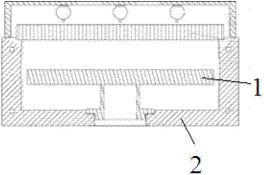
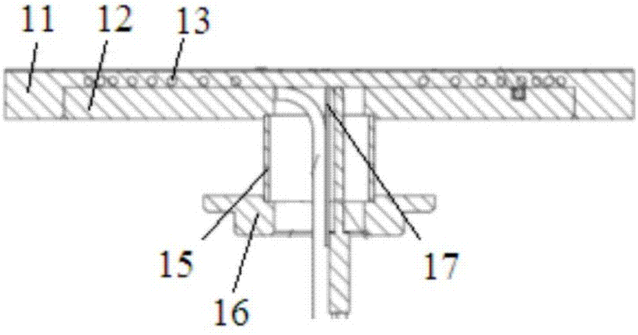
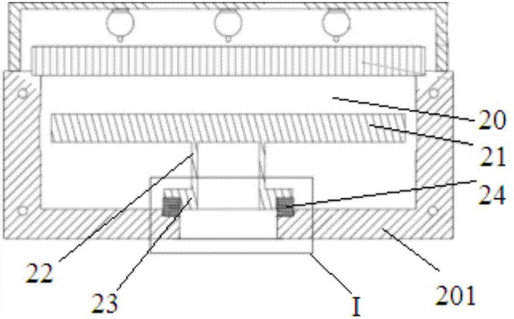
[0038] image 3 A cross-sectional view of a heating chamber provided for an embodiment of the present invention. Figure 4 for image 3 Zoom-in view of the middle I region. Please also refer to image 3 and Figure 4 , the heating chamber 20 includes a heating device and a thermal insulation 24 disposed therein. Wherein, the heating device includes a base 21, a connecting cylinder 22 and a fixed seat 23, wherein the base...
PUM
 Abstract
Description
Claims
Application Information