Display panel, display device and manufacturing method

A display panel and manufacturing method technology, applied in semiconductor/solid-state device manufacturing, semiconductor devices, electrical components, etc., can solve problems such as adverse effects of packaging effects, differences in melting speed, etc., to reduce uneven stress distribution, avoid cracks, improve The effect of package bond strength

Active Publication Date: 2018-01-09
WUHAN TIANMA MICRO ELECTRONICS CO LTD
View PDF4 Cites 4 Cited by
  • Summary
  • Abstract
  • Description
  • Claims
  • Application Information

AI Technical Summary

Problems solved by technology

On the other hand, in the reflective layer of the display panel, the reflectivity is often the same everywhere, which will cause differences in the melting speed of the packaging material under different laser energies, thus adversely affecting the packaging effect

Method used


Image

  • Display panel, display device and manufacturing method
  • Display panel, display device and manufacturing method
  • Display panel, display device and manufacturing method

Examples


Embodiment Construction

[0026] The principles and features of the present application will be further described in detail below in conjunction with the drawings and embodiments. It should be understood that the specific embodiments described here are only used to explain related inventions, rather than to limit the invention. It should also be noted that, for ease of description, only parts related to the invention are shown in the drawings.

[0027] It should be noted that, in the case of no conflict, the embodiments in the present application and the features in the embodiments can be combined with each other. The present application will be described in detail below with reference to the accompanying drawings and embodiments.

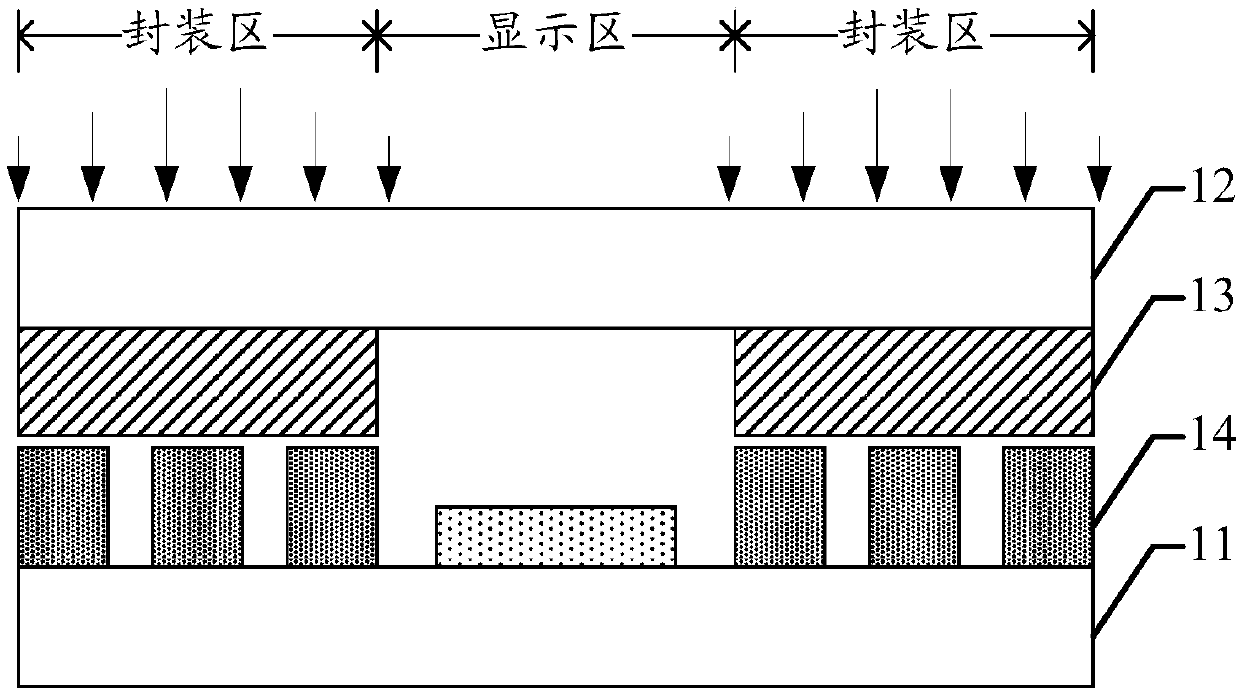
[0028] See figure 1 , which shows a schematic structural diagram of a conventional display panel. Such as figure 1 As shown in , a display panel generally includes a display area and an encapsulation area surrounding the display area. The display area is used to realiz...


PUM


Abstract

The embodiment of the invention discloses a display panel, a display device and a manufacturing method. The display panel comprises a display area, packaging areas surrounding the display area, a substrate and a cover board arranged oppositely to the substrate, wherein a packaging layer is arranged on the surface, toward the substrate, of the cover board in each packaging area; the packaging layers are used for being bonded to the substrate and the cover board after being irradiated by laser light; a plurality of reflecting blocks are formed on the surface, toward the cover board, of the substrate in each packaging area; and the reflectivity of various reflecting blocks is reduced along with an increase of the intensity of the laser light at the positions of various reflecting blocks. According to the display panel, the melting rates of the packaging layers under different intensity of the laser light can tend to be consistent, thereby reducing the defects, such as cracks, caused by astress difference, of the packaging areas. Meanwhile, improvement of the packaging bonding strength between the substrate and the cover board is facilitated, thereby improving the manufacturing yieldof the display panel.

Description

technical field [0001] The present application relates to the field of display technology, in particular to a display panel, a display device and a manufacturing method. Background technique [0002] At present, the packaging principle of the existing display panel is as follows: firstly, a reflective layer is formed on the substrate, and an encapsulation layer is formed on the cover plate; then the cover plate is irradiated with laser light. At this time, the reflective layer can reflect the incident laser light, and the encapsulation material in the encapsulation layer is melted under the action of the laser light and the reflected laser light, so as to realize the encapsulation and bonding of the substrate and the cover plate. [0003] However, the energy distribution of the laser can be regarded as a Gaussian distribution, that is, the energy of the laser at the middle of the energy distribution area is high, and the energy of the laser at both sides of the energy distri...

Claims


Application Information

Patent Timeline
Patent Type & Authority Applications(China)
IPC IPC(8): H01L51/52H01L51/56H01L27/32
Inventor 晏国文
Owner WUHAN TIANMA MICRO ELECTRONICS CO LTD
Why Eureka
Try Eureka