Spliced board process side and board splicing method

A technology of edge and splicing, applied in the field of electronics, can solve the problem that the test results of test strips or test modules cannot truly reflect the graphics unit, uneven thickness of the dielectric layer of PCB splicing, etc., and achieve uniform current density distribution and edge Symmetrical margin, the effect of improving accuracy

Active Publication Date: 2018-01-09
GUANGZHOU FASTPRINT CIRCUIT TECH +2
View PDF6 Cites 8 Cited by
  • Summary
  • Abstract
  • Description
  • Claims
  • Application Information

AI Technical Summary

Problems solved by technology

[0004] Based on this, the present invention is to overcome the defects in the prior art that the thickness of the PCB intermediary layer is uneven due to the design of the PCB, which further leads to the fact that the detection results of the test strip or the test module cannot truly reflect the corresponding value of the graphic unit, and provides a collage process Edge and Jigsaw Method

Method used


Image

  • Spliced board process side and board splicing method
  • Spliced board process side and board splicing method
  • Spliced board process side and board splicing method

Examples


Embodiment Construction

[0034] In order to make the object, technical solution and advantages of the present invention clearer, the present invention will be further described in detail below in conjunction with the accompanying drawings and specific implementation methods. It should be understood that the specific embodiments described here are only used to explain the present invention, and do not limit the protection scope of the present invention.

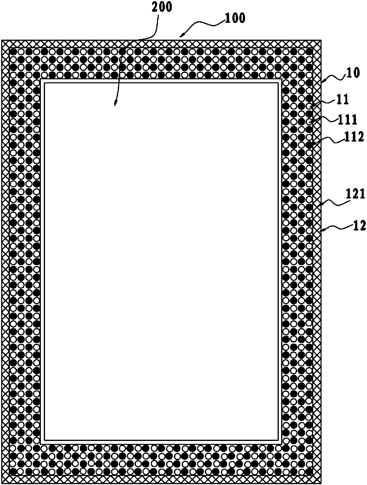
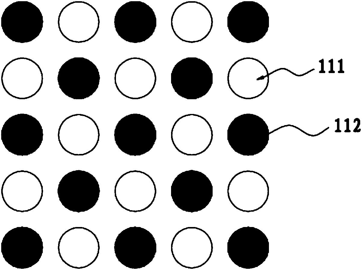
[0035] Such as figure 1 A panel process edge 100 as shown is arranged on the periphery of the graphic unit 200 of the circuit board, including: at least two layers of process edges 10 stacked, each layer of process edge 10 is provided with a balance copper point 11, and each layer The residual copper ratio of the process edge 10 is the same as the residual copper ratio of the pattern unit 200 of the corresponding layer.

[0036] The jigsaw process edge 100 of this embodiment has the same laminated layer as the jigsaw graphics unit 200, and the jigsaw...


PUM


Abstract

The invention discloses a spliced board process side and a board splicing method. The spliced board process side is arranged at the periphery of the pattern units of a circuit board. The spliced boardprocess side comprises at least two layers of laminated process sides. Each layer of process side is provided with balance copper points, and the residual copper rate of each layer of process side isthe same with the residual copper rate of the pattern units of the corresponding layer. The spliced board of the board splicing method comprises the spliced board process side and the pattern units and test strips or test modules which are arranged in the spliced board process side. According to the spliced board process side, the residual copper rate of each layer is the same with the residual copper rate of the pattern units of the corresponding layer so that the consistency of the dielectric layer thickness of the spliced board process side and the pattern units after lamination and glue filling can be guaranteed, the board thickness consistency of the spliced board can be enhanced, the current density distribution of the spliced board process side and the pattern units in electroplating is ensured to be more uniform, the accuracy of the test result of the test strips or the test modules arranged in the process side can be enhanced and the relevant real value of the pattern units can be effectively represented.

Description

technical field [0001] The present invention relates to the field of electronics, and more specifically, to a jigsaw process edge and a jigsaw method. Background technique [0002] The uniformity of the thickness of the PCB dielectric layer has a certain impact on the performance of the PCB. For example, as the PCB tends to be thinner and shorter, the thickness of the dielectric layer in the PCB is getting smaller and smaller, so that the control of the uniformity of the dielectric layer thickness has a great impact on the impedance. The impact is growing. For PCBs with impedance control requirements, the current common practice is to design impedance test strips or test modules at the edge of the PCB panel to simulate the impedance in the unit. The impedance of the impedance test strips or test modules can be detected quickly and conveniently. To accurately judge the impedance control of the PCB. However, due to the large differences between the graphics of the impedance ...

Claims


Application Information

Patent Timeline
Patent Type & Authority Applications(China)
IPC IPC(8): H05K1/02H05K1/14
CPCH05K1/02H05K1/14
Inventor 程柳军李艳国陈蓓
Owner GUANGZHOU FASTPRINT CIRCUIT TECH
Why Eureka
Try Eureka