A self-cleaning flexible conductive circuit and its preparation method

A flexible conductive and self-cleaning technology, applied in the field of flexible microelectronics, can solve the problems of low bonding strength, poor line edge selectivity, poor reliability of conductive lines, etc., and achieve the effects of simple method, improved bonding strength, and good reliability performance.

Active Publication Date: 2019-09-13
HUAZHONG UNIV OF SCI & TECH
View PDF4 Cites 0 Cited by
  • Summary
  • Abstract
  • Description
  • Claims
  • Application Information

AI Technical Summary

Problems solved by technology

[0005] Aiming at the above defects or improvement needs of the prior art, the present invention provides a self-cleaning flexible conductive circuit and its preparation method, thereby solving the problems of poor reliability, low bonding strength, low resolution and circuit defects of the conductive circuit prepared in the prior art. Technical issues with poor edge selectivity

Method used


Image

  • A self-cleaning flexible conductive circuit and its preparation method

Examples


preparation example Construction

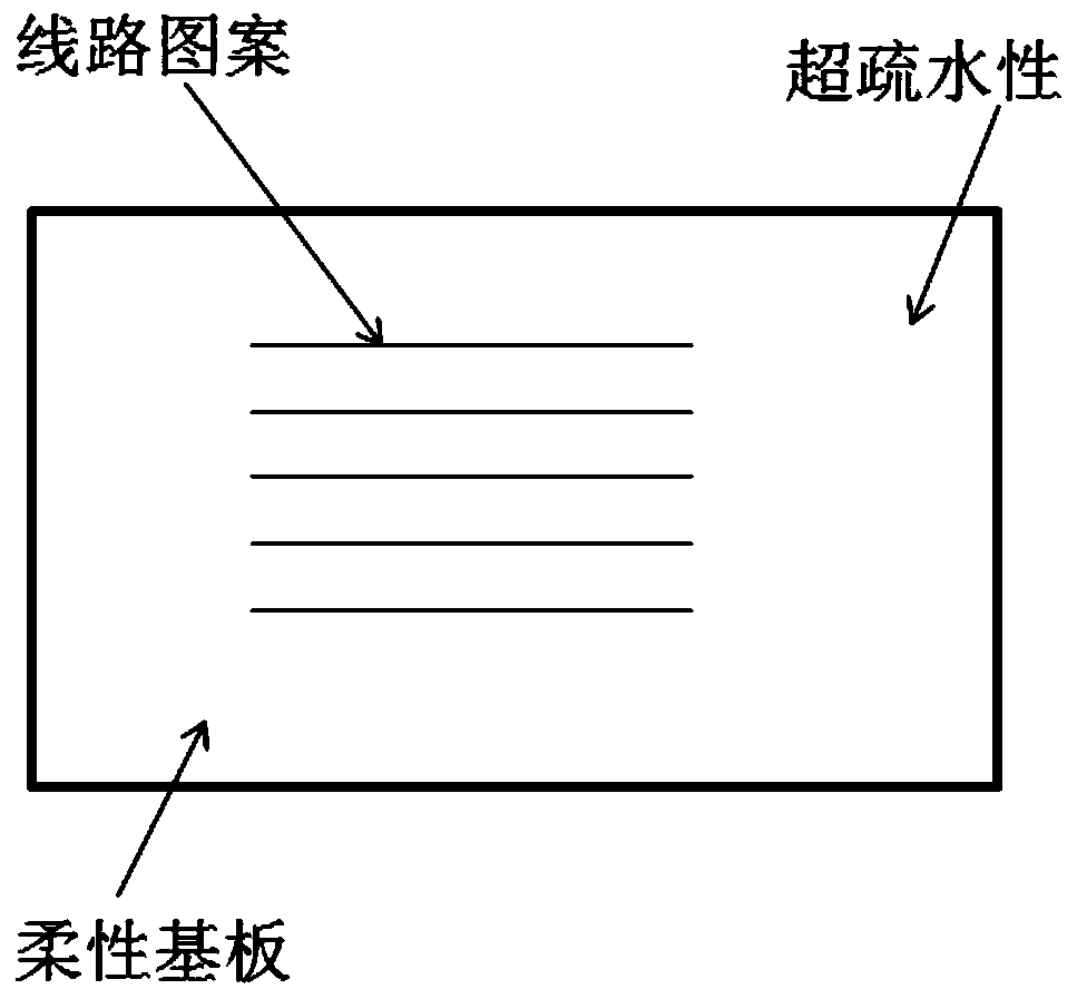
[0030] Such as figure 1 Shown, a kind of preparation method of self-cleaning flexible conductive circuit comprises:

[0031] (1) Use a nanosecond pulse laser with a wavelength of 256nm-1064nm and a single pulse energy of 0.1μJ-20μJ to etch and scan the cleaned flexible substrate. When the content of hydrophilic groups on the surface of the flexible substrate is reduced and a micro-protrusion structure is formed, According to the Cassie and Baxter wetting model, the surface of the flexible substrate exhibits superhydrophobicity;

[0032] (2) Using the ultraviolet pulse laser with a single pulse energy of 1μJ-50μJ to etch the circuit pattern on the superhydrophobic flexible substrate, the content of hydrophilic groups on the surface of the area after the laser secondary action increases and forms a groove structure, According to the Wenzel wetting model, the circuit pattern is superhydrophilic;

[0033] (3) Coat the surface of the flexible substrate after the laser treatment i...

Embodiment 1

[0037] A nanosecond pulse laser with a wavelength of 355 nm and a single pulse energy of 0.1 μJ was used to etch and scan the cleaned polyimide flexible substrate, so that the surface of the substrate appeared superhydrophobic. The ultra-hydrophilic circuit pattern was etched on the super-hydrophobic substrate by using an ultraviolet pulse laser with a single pulse energy of 1 μJ again. A solution containing silver ammonia ions at a concentration of 0.1 mol / L was coated on the surface of the substrate after laser treatment, and after 5 minutes, the substrate was cleaned with deionized water and dried. Finally, put the base material adsorbed with silver ammonia ions into the chemical gold plating solution, the chemical gold plating solution is a common commercial plating solution, the temperature is controlled at 50° C., and the gold plating time is 50 minutes. After completion, take it out, wash it, and dry it to obtain a self-cleaning flexible conductive circuit.

Embodiment 2

[0039]A nanosecond pulse laser with a wavelength of 1064 nm and a single pulse energy of 0.5 μJ was used to etch and scan the clean polyethylene terephthalate flexible substrate, making the surface of the substrate superhydrophobic. The ultra-hydrophilic circuit pattern was etched on the super-hydrophobic substrate by using an ultraviolet pulse laser with a single pulse energy of 2 μJ again. A solution containing silver ions at a concentration of 0.5 mol / L was coated on the surface of the substrate after laser treatment, and after 10 minutes, the substrate was cleaned with deionized water and dried. Finally, the substrate with the silver ions adsorbed is put into the electroless copper plating solution, which is a common commercial plating solution, the temperature is controlled at 50° C., and the copper plating time is 50 minutes. After completion, take it out, wash it, and dry it to obtain a self-cleaning flexible conductive circuit.


PUM


Abstract

The invention discloses a self-cleaning flexible conductive circuit and a fabrication method thereof. The fabrication method comprises the steps of etching, scanning and cleaning a flexible substratewith laser having wavelength being 256-1,064 nanometers and single pulse energy being 0.1-20 micro joules so that a surface of the flexible substrate shows super-hydrophobicity; etching a circuit pattern on the super-hydrophobic flexible substrate with laser having single pulse energy being 1-50 micro joules again, wherein the circuit pattern shows the super-hydrophobicity; coating an activating agent on the surface of the flexible substrate subjected to laser processing, and rapidly wetting the circuit pattern by the activating agent; and placing the flexible substrate which is rapidly wettedby the activating agent in a chemical plating liquid for deposition of a metal layer so as to obtain the self-cleaning flexible conductive circuit. The circuit between conductive circuits shows the super-hydrophobicity, has the advantages of dust prevention, damp prevention, good circuit reliability, high bonding strength, high resolution and good circuit edge selectivity.

Description

technical field [0001] The invention belongs to the field of flexible microelectronics, and more specifically relates to a self-cleaning flexible conductive circuit and a preparation method thereof. Background technique [0002] Flexible conductive circuits are widely used in the field of microelectronics such as molded interconnect devices (MID), flexible circuit boards (FPC), and radio frequency identification (RFID). With the development of microelectronics technology, people put forward higher requirements for the reliability, refinement and environmental protection of the flexible circuit. At present, the preparation of flexible electronic circuits mainly adopts a subtractive process, that is, covering the entire flexible substrate with a metal layer, and then forming a conductive circuit through steps such as masking, exposure, development, and chemical etching. However, this method has disadvantages such as complex process, serious waste of materials, pollution to th...

Claims


Application Information

Patent Timeline
Patent Type & Authority Patents(China)
IPC IPC(8): H05K3/18
Inventor 刘建国杜琦峰曾晓雁
Owner HUAZHONG UNIV OF SCI & TECH
Why Eureka
Try Eureka