Preparation method of trench type device

A trench type and trench technology, which is applied in the manufacture of semiconductor/solid-state devices, semiconductor devices, electrical components, etc., can solve the problems of lithography capacity limitation and limit the development of trench MOSFET devices, etc., to reduce the on-resistance, The effect of increasing density

Inactive Publication Date: 2018-01-12
CHINA RESOURCES MICROELECTRONICS (CHONGQING) CO LTD
View PDF3 Cites 0 Cited by
  • Summary
  • Abstract
  • Description
  • Claims
  • Application Information

AI Technical Summary

Problems solved by technology

At present, the mature process is to form the source contact hole of the active region of the device through photolithography, but due to the limitation of photolithography capability, the line width of the cell cannot be reduced forever, which limits the development of trench MOSFET devices.

Method used


Image

  • Preparation method of trench type device
  • Preparation method of trench type device
  • Preparation method of trench type device

Examples


preparation example Construction

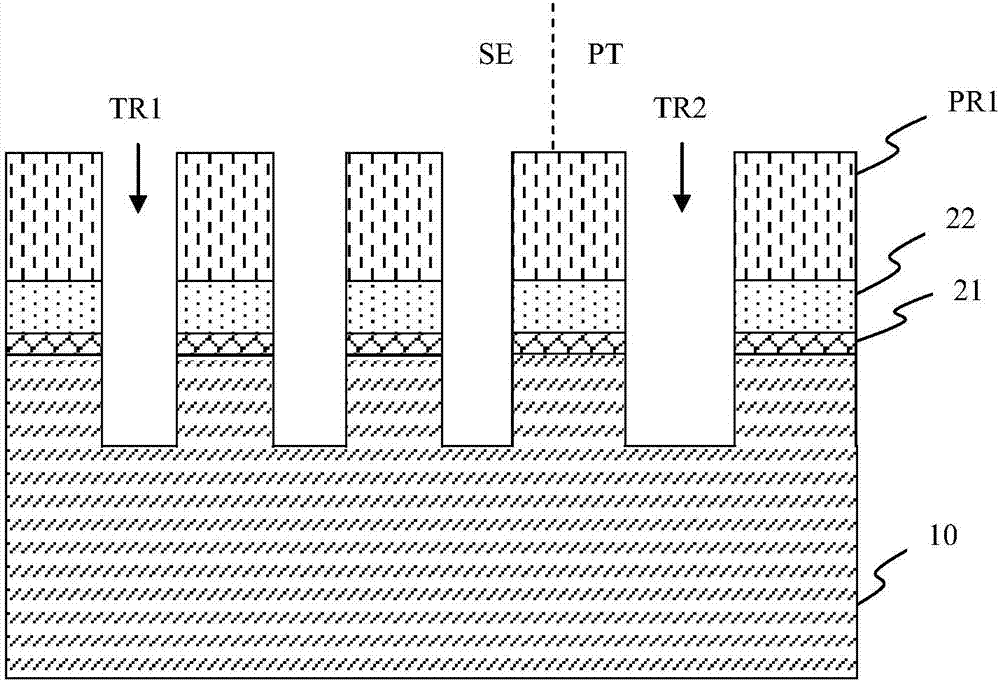
[0035] In a preferred embodiment, as Figure 1-9 As shown, a method for preparing a trench device is proposed, which may include:

[0036] Step S1, providing a substrate 10 including a cell region CE and a protection region PT, and sequentially depositing a first dielectric layer 21 and a second dielectric layer 22 on the upper surface of the substrate 10;

[0037] Step S2, etching the upper surface of the second dielectric layer 22 into the substrate 10 to form a plurality of first trenches TR1 in the cell region CE and at least one second trench TR2 in the protection region PT;

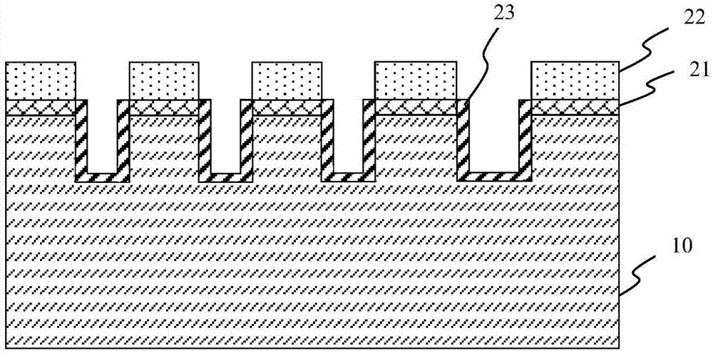
[0038] Step S3, covering the sidewalls and bottoms of the first trench TR1 and the second trench TR2 with a third dielectric layer 23;

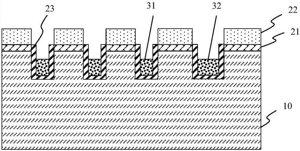
[0039] Step S4, preparing the first conductive layer 31 in the first trench TR1 covering the third dielectric layer 23, and preparing the second conductive layer 32 in the second trench TR2 covering the third dielectric layer 23, and the first conductive The upper...


PUM


Abstract

The invention relates to the technical field of semiconductors, and particularly relates to a preparation method of a trench type device. A dielectric layer grows on the sidewall and the bottom of thetrench of a cellular area. After the formation of a body region structure and a source electrode, a dielectric layer filling trench is prepared. The area between the dielectric layer of the cellulararea to the upper surface of the body region structure is etched, so that the upper surface of the body region structure in the cellular area is exposed. The dielectric layer in a protection region isetched to form a contact hole in connection with an electrically conductive layer. During the implantation process, the exposed upper surface of the body region structure in the cellular area is processed to form an ohmic contact structure. A first metal layer is filled inside the contact hole, and a second metal layer is used for connecting and covering the source electrode and the upper surfaceof the ohmic contact structure so as to form the gate metal and the source metal respectively. By adopting the above technical scheme of the invention, the line width of a cellular trench of the trench type device prepared by the invention can be lower than 1 micron. Therefore, the density of the cellular trench is increased, and the source and drain conduction resistance of the trench type device is reduced.

Description

technical field [0001] The invention relates to the technical field of semiconductors, in particular to a method for preparing a trench device. Background technique [0002] MOSFET (Metal-Oxide-Semiconductor Field-Effect Transistor Metal-Oxide-Semiconductor Field-Effect Transistor, referred to as MOSFET) is a field-effect transistor that can be widely used in analog circuits and digital circuits. [0003] For trench MOSFET devices, the source-drain on-resistance is an important parameter. Low on-resistance can greatly reduce the switching loss of the device, which has always been the goal pursued by people. Therefore, many new device structures have been designed, and many improvements have been made to the process to reduce the on-resistance of the source and drain. Reducing the line width of trench-type device cells and increasing the cell density is a very effective way to reduce the source-drain on-resistance. At present, the mature process is to form the source conta...

Claims


Application Information

Patent Timeline
Patent Type & Authority Applications(China)
IPC IPC(8): H01L21/336H01L29/78H01L29/06
Inventor 陈雪萌王艳颖杨林森
Owner CHINA RESOURCES MICROELECTRONICS (CHONGQING) CO LTD
Why Eureka
Try Eureka