Radio frequency ldmos device and manufacturing method thereof

A device and radio frequency technology, which is applied in the field of semiconductor integrated circuit manufacturing, can solve the problems of unfavorable Coss drop, drop, and the breakdown voltage of the drift region 103 cannot be fully depleted.

Active Publication Date: 2018-04-17
SHANGHAI HUAHONG GRACE SEMICON MFG CORP
View PDF6 Cites 0 Cited by
  • Summary
  • Abstract
  • Description
  • Claims
  • Application Information

AI Technical Summary

Problems solved by technology

To keep RDSON low, it is necessary to increase the doping concentration of the drift region 103 as much as possible, but this may cause the drift region 103 to not be completely depleted when a high voltage is applied to the drain region 106, resulting in a drop in breakdown voltage
In addition, the main factor restricting the decline of Coss is the junction capacitance from the drift region 103 to the silicon substrate 101. If the concentration of the drift region 103 increases, the junction capacitance will also increase, which is also not conducive to the decline of Coss.
Therefore, the two parameters of RDSON and Coss are mutually restricted, and the existing device structure cannot simply increase the concentration of the drift region to reduce both of them at the same time, so the device characteristics of the existing RF LDMOS are difficult to achieve excellent performance

Method used


Image

  • Radio frequency ldmos device and manufacturing method thereof
  • Radio frequency ldmos device and manufacturing method thereof
  • Radio frequency ldmos device and manufacturing method thereof

Examples


Embodiment 2

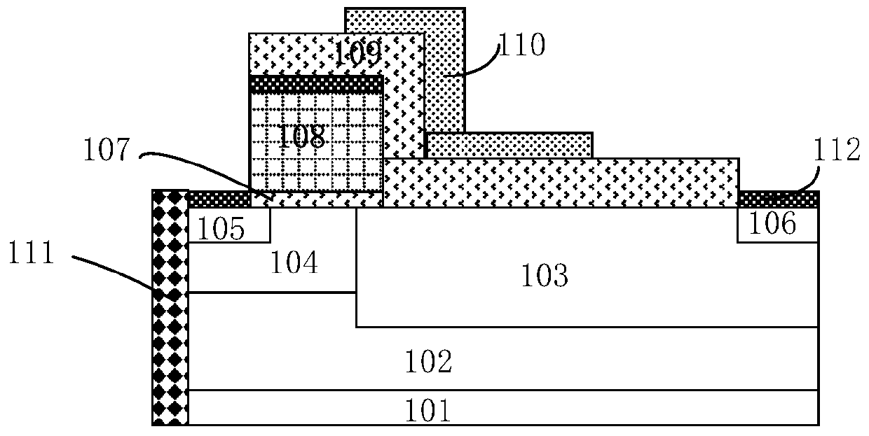
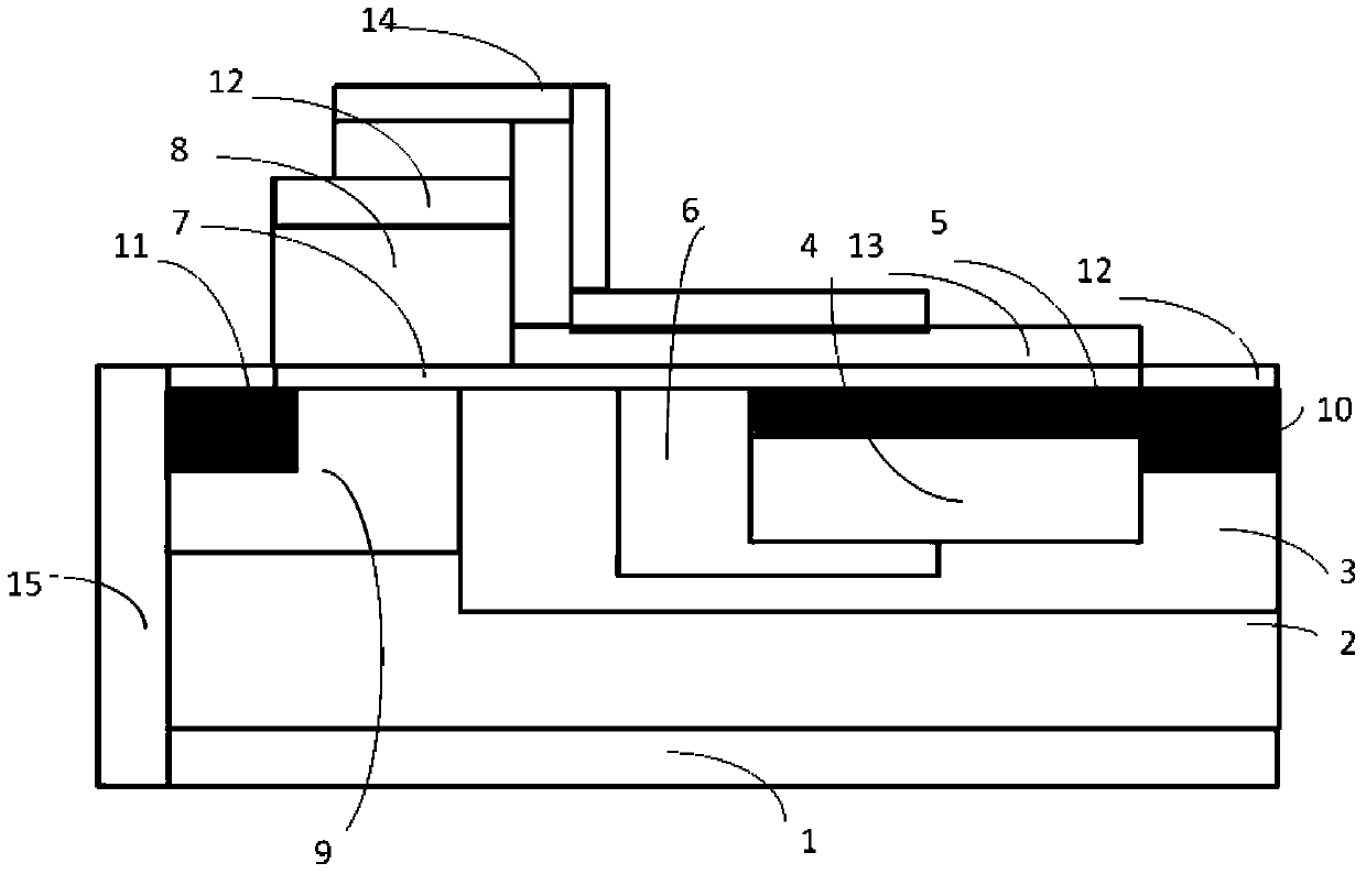
[0110] The second method of the embodiment of the present invention is also used to manufacture such as figure 2 In the device of the embodiment of the present invention shown, the first drift region 3 is formed by photolithography instead of the self-alignment process in the first method of the present invention, while the self-alignment process is used in the second method of the present invention forming the first drift region 3, such as figure 2 As shown, the manufacturing method of the radio frequency LDMOS device of the second embodiment of the present invention includes the following steps:

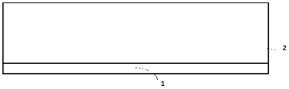
[0111] Step 1: epitaxially grow on the surface of the heavily doped silicon substrate 1 of the first conductivity type to form a silicon epitaxial layer 2 doped with the first conductivity type. Preferably, the doping concentration of the silicon substrate 1 is greater than 1e20cm -3 .

[0112] Step 2, growing a gate dielectric layer 7 on the surface of the silicon epitaxial l...


PUM


Abstract

The invention discloses a radio frequency LDMOS device. The drift region is a non-uniformly doped structure, and the distance between the channel and the drain region is sequentially the first, third and second drift regions. The doping concentration of the first drift region is the lowest, and the energy Reduce the electric field intensity and hot carrier effect near the channel region to improve the reliability of the device; the second drift region adopts a higher doping concentration, which can reduce the on-resistance of the device; the reflection formed on the surface of the second drift region The doped cover layer can effectively help deplete the drift region, reduce the output capacitance of the device, and prevent the charge and interface state of the shielding dielectric layer not covered by the Faraday shielding layer from affecting the device, making the device characteristics more stable. The second drift region is a transition region, which can further increase the driving current of the device and reduce the on-resistance of the device without affecting the reliability and output capacitance of the device. The invention also discloses a manufacturing method of the radio frequency LDMOS device.

Description

technical field [0001] The invention relates to the field of semiconductor integrated circuit manufacturing, in particular to a radio frequency LDMOS device; the invention also relates to a method for manufacturing the radio frequency LDMOS device. Background technique [0002] RF Lateral Field Effect Transistor (RF LDMOS) is a common device used in RF base stations and broadcasting stations. High breakdown voltage, low source-drain on-resistance (RDSON) and low source-drain parasitic capacitance (Coss) are device characteristics that RF LDMOS must have. In order to minimize the parasitic capacitance between the source region, the channel and the substrate, a heavily doped substrate material and a lightly doped epitaxial layer are usually used, and tungsten deep contact holes are used to connect the source region, channel, and substrate. epitaxial layer and substrate. like figure 1 Shown is a schematic structural diagram of an existing radio frequency LDMOS device. Taking...

Claims


Application Information

Patent Timeline
Patent Type & Authority Patents(China)
IPC IPC(8): H01L29/78H01L29/36H01L21/336
Inventor 钱文生
Owner SHANGHAI HUAHONG GRACE SEMICON MFG CORP
Why Eureka
Try Eureka