Fabrication method of superjunction device

A manufacturing method and super junction technology, which are applied in semiconductor/solid-state device manufacturing, semiconductor devices, electrical components, etc., can solve problems such as the increase in the concentration of the P region, the smaller the N-type column, and the reduction of source-drain conductance. The effect of on-resistance

Active Publication Date: 2018-10-26
SHANGHAI HUAHONG GRACE SEMICON MFG CORP
View PDF1 Cites 0 Cited by
  • Summary
  • Abstract
  • Description
  • Claims
  • Application Information

AI Technical Summary

Problems solved by technology

[0005] No matter which method is used, it will cause a problem, that is, after the P-type column is formed, due to the inevitable thermal process in the process, and the P-type impurity of the P-type column generally adopts boron (B) element, the thermal process It will cause the B element in the P area, that is, the P-type column, to diffuse to the N area, resulting in a larger concentration of the P area, and a smaller N area, that is, the N-type column; at the same time, in order to obtain a device with a higher breakdown voltage Performance, will choose a relatively large epitaxy of RS, which eventually leads to a larger source-drain on-resistance (RDSON) than expected

Method used


Image

  • Fabrication method of superjunction device
  • Fabrication method of superjunction device
  • Fabrication method of superjunction device

Examples


Embodiment Construction

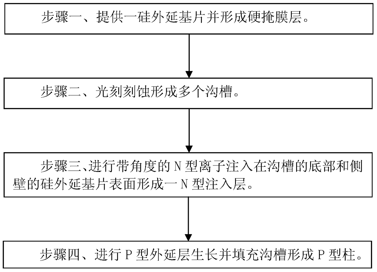
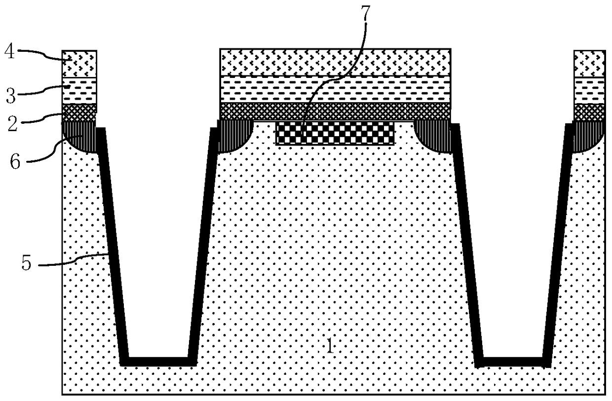
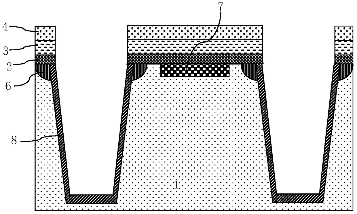
[0039] Such as figure 1 Shown is the flow chart of the method of the embodiment of the present invention; Figure 2A to Figure 2C As shown, it is a device structure diagram in each step of the method of the embodiment of the present invention; the super junction device in the embodiment of the present invention is illustrated by taking a super junction N-type MOSFET device with a working voltage of 600V and a current of 5 amps as an example, and the implementation of the present invention The manufacturing method of example superjunction device comprises following manufacturing steps:

[0040] Step 1, such as Figure 2A As shown, an N-type lightly doped silicon epitaxial substrate 1 is provided. In the embodiment of the present invention, the silicon epitaxial substrate 1 is a zone-melted silicon epitaxial substrate. The silicon epitaxial substrate 1 has a resistivity of 1 ohm·cm to 30 ohm·cm, and a thickness of more than 700 microns.

[0041] A JFET implantation process i...


PUM


Abstract

The invention discloses a manufacturing method of a super junction device. The method comprises the following steps that 1, a silicon epitaxial substrate is provided, and in addition, a hard mask layer is formed; 2, a plurality of grooves are formed through photoetching; 3, N type ions with angles are injected onto the surfaces of the bottom and the silicon epitaxial substrate arranged at the bottom and the side wall of the grooves for forming an N type ion injection layer; 4, P type epitaxial layer growth is carried out, and in addition, the grooves are filled to form P type columns. The manufacturing method has the advantage that the source drain conduction resistance of the device can be reduced.

Description

technical field [0001] The invention relates to a manufacturing process method of a semiconductor integrated circuit, in particular to a manufacturing method of a super junction device. Background technique [0002] Super Junction is composed of P-type pillars and N-type pillars arranged alternately. The carriers between P-type pillars and N-type pillars are easy to deplete each other to improve the breakdown voltage of the device. In the prior art, it is common There are two methods of super knot operation: [0003] A method of matching multiple ion implantations for multiple epitaxy, and then connecting the multiple-implanted P-type wells (Well) into a P-type column through an annealing drive in method. [0004] Another method is to grow one or two layers of epitaxy first, and hollow out the epitaxial layer that needs to be filled with P-type columns by digging trenches to form trenches, and then fill the trenches with P-type epitaxy to form P-type columns. . [0005] N...

Claims


Application Information

Patent Timeline
Patent Type & Authority Patents(China)
IPC IPC(8): H01L21/336H01L21/266
CPCH01L21/266H01L29/0603H01L29/0684H01L29/66477
Inventor 姚亮王飞顾文炳
Owner SHANGHAI HUAHONG GRACE SEMICON MFG CORP
Why Eureka
Try Eureka