Storage, forming method thereof and semiconductor device

A memory and conductor technology, applied in the field of memory and its formation, semiconductor devices, can solve problems such as position deviation

Active Publication Date: 2018-01-19
CHANGXIN MEMORY TECH INC
View PDF4 Cites 5 Cited by
  • Summary
  • Abstract
  • Description
  • Claims
  • Application Information

AI Technical Summary

Problems solved by technology

[0005] The purpose of the present invention is to provide a method for forming a memory, so as to solve the problem of easy position deviation when the node contact window is directly defined by the photolithography process in the existing forming method, and it is also beneficial to improve the arrangement of the capacitor Intensity

Method used


Image

  • Storage, forming method thereof and semiconductor device
  • Storage, forming method thereof and semiconductor device
  • Storage, forming method thereof and semiconductor device

Examples


Embodiment 1

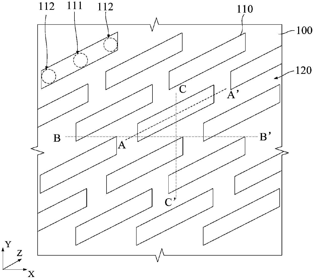
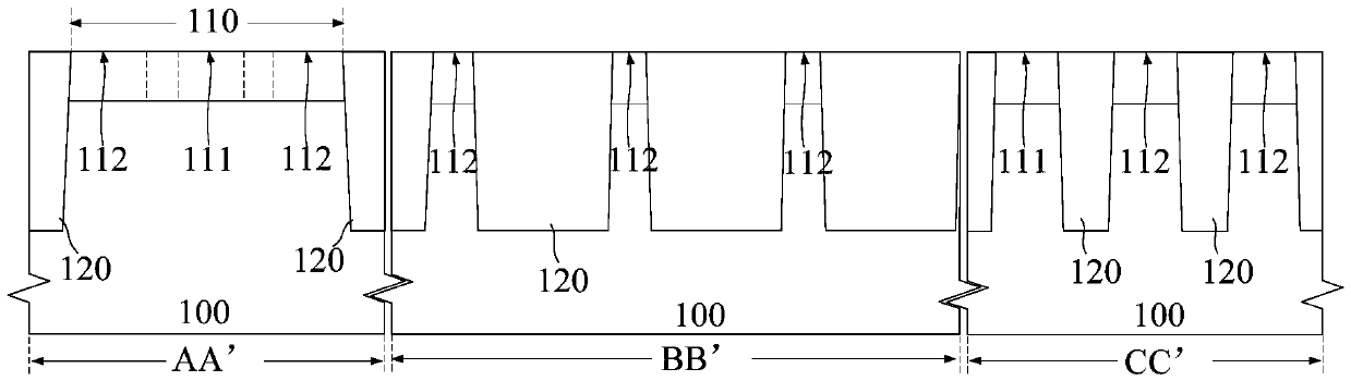
[0116] Figure 2a is a top view of the memory forming method in Embodiment 1 of the present invention when step S110 is executed, Figure 2b for Figure 2a The shown cross-sectional views of the memory forming method in Embodiment 1 of the present invention along the directions AA', BB' and CC when step S110 is executed.

[0117] In step S110, refer to Figure 2a with Figure 2b As shown, a substrate 100 is provided, and a plurality of active regions 110 are formed in the substrate 100, and a first region for forming a bit line contact region 111 and a plurality of active regions 110 are defined in the active region 110. For forming the second region of the node contact region 112 , a plurality of the second regions are distributed on both sides of the first region.

[0118] In this embodiment, the active region 110 extends obliquely relative to the first direction (Y direction), and a plurality of the first regions extend in the extending direction of the active region 11...

Embodiment 2

[0185] Another object of the present invention is to provide a memory, which utilizes a plurality of first isolation barriers and a plurality of second isolation barriers to define node contact windows corresponding to node contact regions, and the second isolation barrier utilizes A second isolation line makes the top surface of the second isolation barrier higher than the top surface of the first isolation barrier, so that a node contact extending along the extension direction of the second isolation barrier can be formed.

[0186] Figure 12ais a top view of the memory in Embodiment 2 of the present invention, Figure 12b for Figure 12a The shown cross-sectional views of the memory in Embodiment 2 of the present invention along the directions AA', BB' and CC. combine Figure 12a with Figure 12b As shown, the memory includes:

[0187] A substrate 100, a plurality of active regions 110 are formed in the substrate 100, a bit line contact region 111 and a plurality of no...

Embodiment 3

[0200] Based on the memory and its forming method described above, the present invention also provides a semiconductor device. The semiconductor device includes:

[0201] a substrate in which a plurality of first contact regions are formed;

[0202] a plurality of first isolation barriers, formed by a plurality of first isolation lines formed on the substrate, and extending in a first direction;

[0203] a plurality of second isolation barriers formed on the substrate and extending along a second direction, the first isolation barriers and the second isolation barriers intersecting on the surface of the substrate to jointly define a plurality of A contact window, each of the first contact regions corresponds to one of the contact windows, and the second isolation barrier includes a second isolation line, so as to use the second isolation line relative to the first isolation line in the a thickness difference on the substrate such that the top surface of the second isolation ...


PUM


Abstract

The invention provides a storage, a forming method thereof and a semiconductor device. A word line mask which defines a word line conductor is used for forming a first isolation barrier in an autocollimation manner, and a thickening layer is formed so as to increase the thickness of a forming substrate of a second isolation barrier so that the top surface of the second isolation barrier in the forming substrate can be higher than the top surface of the first isolation barrier. Therefore, not only can the crossed first isolation barrier and second isolation barrier be used for defining a node contact window, and accordingly, the problem of displacement deviation caused by the photolithography technique can be eliminated; but also the lower top surface of the first isolation barrier is usedso as to realize extension of the top in contact with the nodes and adjust the arrangement manner of a plurality of nodes on the contact surface of the nodes and a capacitor, and the arrangement density of the capacitor can be further optimized.

Description

technical field [0001] The invention relates to the technical field of semiconductors, in particular to a memory, a method for forming the same, and a semiconductor device. Background technique [0002] A memory typically includes a storage capacitor for storing charge representing stored information and a storage transistor connected to the storage element. An active region, a drain region and a gate are formed in the memory transistor, the gate is used to control the flow of current between the source region and the drain region, and is connected to a word line conductor, and the source region is used to form The bit line contact area is used to connect to the bit line conductor through the bit line contact, and the drain area is used to form a node contact area to connect to the storage capacitor through a node contact. [0003] At present, when forming a node contact, generally, a photolithography process is used to directly define the formation area of ​​the node conta...

Claims


Application Information

Patent Timeline
IPC IPC(8): H01L27/11568
Inventor 不公告发明人
Owner CHANGXIN MEMORY TECH INC
Why Eureka
Try Eureka