Resin composition for photo-semiconductor, method for producing same, and photo-semiconductor device
A resin composition, optical semiconductor technology, applied in the direction of semiconductor devices, electrical components, circuits, etc., can solve the problems of large transmittance changes, lack of productivity, increased brightness changes, etc., to achieve excellent molding workability, sealing work Excellent performance and good productivity
- Summary
- Abstract
- Description
- Claims
- Application Information
AI Technical Summary
Problems solved by technology
Method used
Image
Examples
Embodiment 1
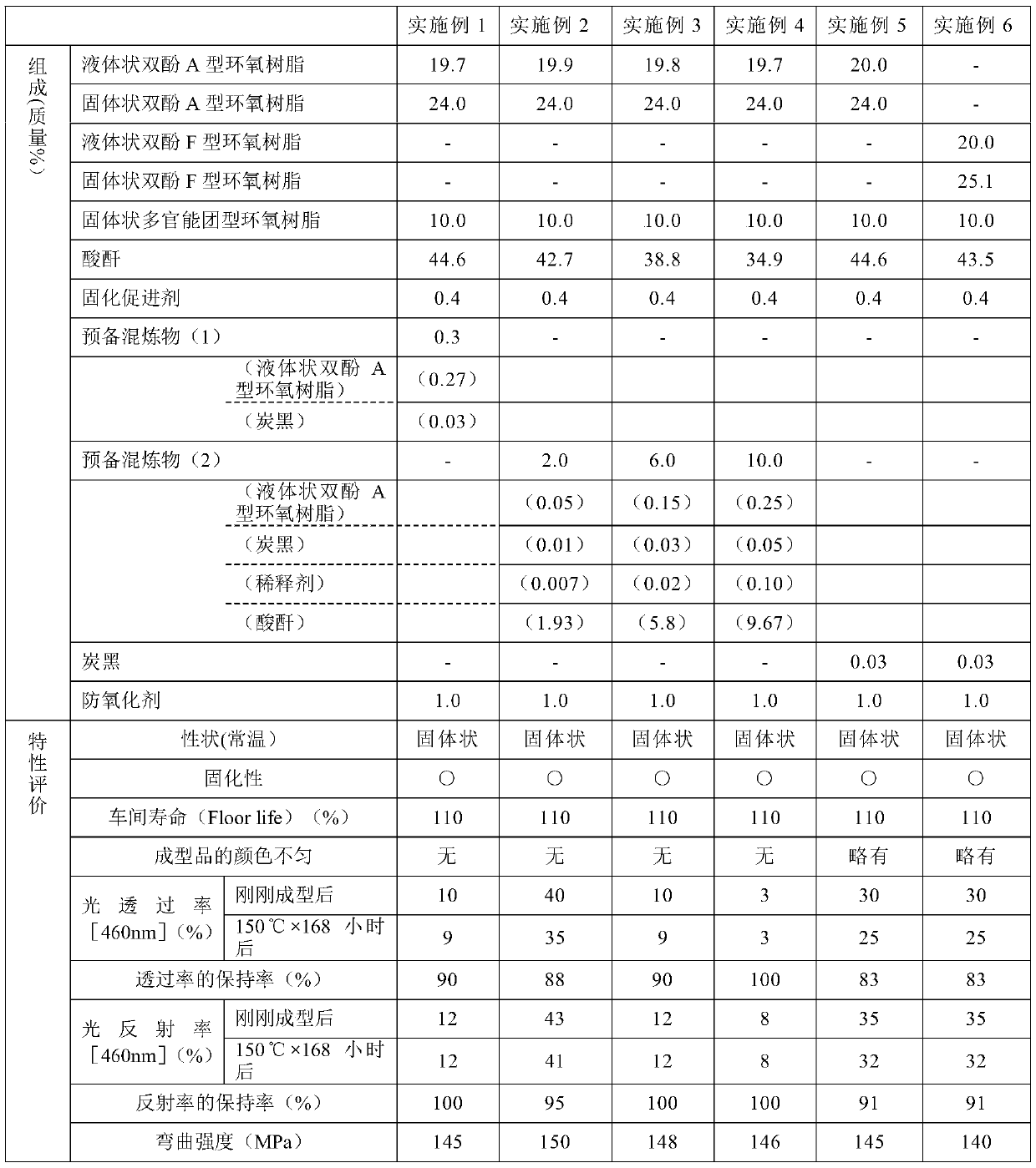
[0061] In order to obtain the compounding amount of the composition shown in Table 1, first, the above-mentioned pre-kneaded product (1), liquid bisphenol A epoxy resin ("YD-8125") at room temperature, bisphenol A type epoxy resin ("YD-8125") solid at room temperature, Phenol A type epoxy resin (produced by Mitsubishi Chemical Co., Ltd., trade name "Epikote 1002" ("Epikote 1002")), a trifunctional epoxy resin with a triazine skeleton in a solid state at room temperature (Nissan Chemical Industry Co., Ltd. ), product name "TEPIC-S"), liquid acid anhydride at room temperature (manufactured by Shin Nippon Chemical Co., Ltd., product name "RIKACID MH-700" ("RIKACID MH-700")), and di Butylated hydroxytoluene (BHT) is mixed at a temperature of 70°C by a universal mixer, and secondly, in the mixture, dimethyl tributylphosphonium phosphate (manufactured by Nippon Chemical Industry Co., Ltd.) is added as a curing accelerator , trade name "ヒシコーリン PX-4MP" ("HISHICOLINPX-4MP")), further k...
Embodiment 2~4
[0062] (Examples 2-4, Comparative Examples 1-4)
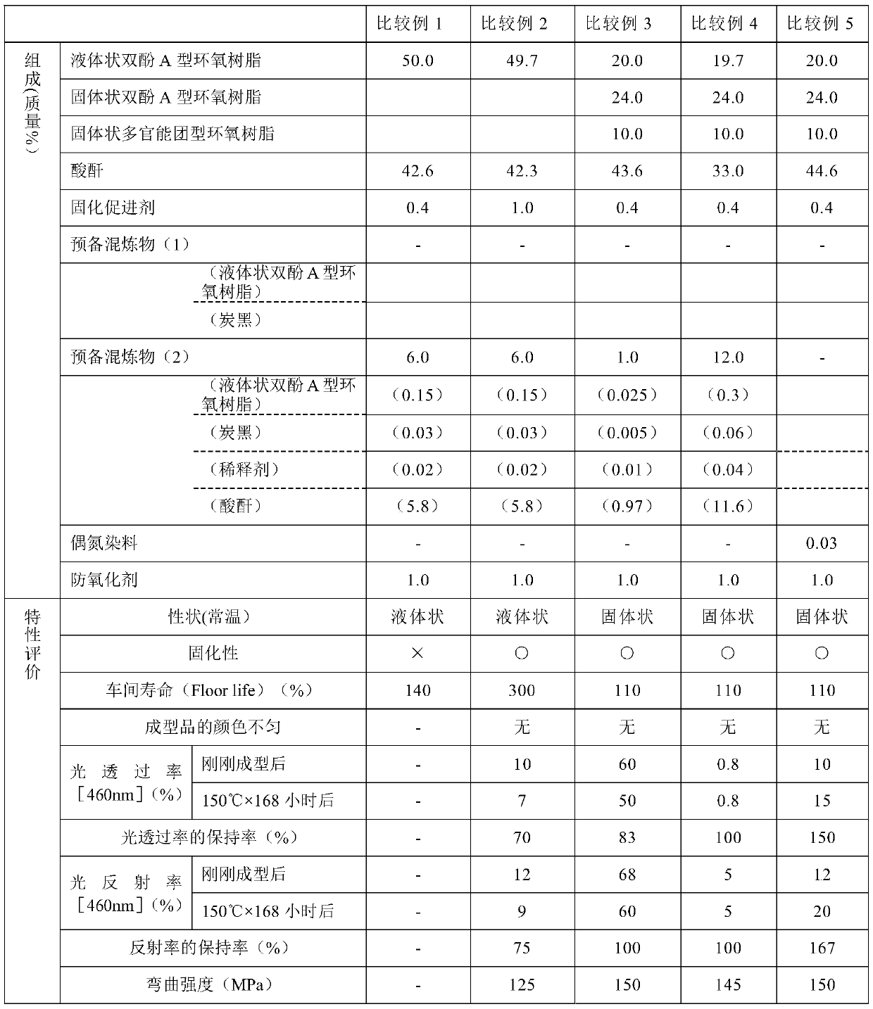
[0063] Except that the pre-kneaded product (2) was used instead of the pre-kneaded product (1), and the compounding amount was set so that the compounding amount of each component became the composition shown in Tables 1 and 2, it was the same as in Example 1. operation to obtain a resin composition for optical semiconductors.
Embodiment 5
[0065] Except having mixed carbon black and another component as it was without using the pre-kneaded product, it carried out similarly to Example 1, and obtained the resin composition for optical semiconductors of the composition similar to Example 1.
PUM
| Property | Measurement | Unit |
|---|---|---|
| particle size | aaaaa | aaaaa |
| particle diameter | aaaaa | aaaaa |
| particle diameter | aaaaa | aaaaa |
Abstract
Description
Claims
Application Information

