Resin composition for optical semiconductor, manufacturing method thereof, and optical semiconductor device

A resin composition and optical semiconductor technology, applied in the direction of semiconductor devices, electrical components, circuits, etc., can solve problems such as lack of productivity, large transmittance changes, and increased brightness changes, and achieve excellent sealing workability and molding operations Excellent performance and good productivity

Inactive Publication Date: 2018-01-23
KYOCERA CORP
View PDF5 Cites 4 Cited by
  • Summary
  • Abstract
  • Description
  • Claims
  • Application Information

AI Technical Summary

Problems solved by technology

However, for the sealing method using a two-component type sealing material, it lacks the aforementioned productivity.
Correspondingly, in transfer molding and compression molding using a solid sealing material with high productivity, solidification occurs when the mixing / kneading time increases, so it is difficult to suppress the segregation of the colorant
[0006] In addition, although the above-mentioned segregation problem can be solved if an organic dye is used as a colorant, due to its lack of heat resistance, especially in the case of adding a small amount, the transmittance changes greatly after the heat history. In the case of sealing a light-emitting element with it, the change in luminance increases

Method used


Image

  • Resin composition for optical semiconductor, manufacturing method thereof, and optical semiconductor device
  • Resin composition for optical semiconductor, manufacturing method thereof, and optical semiconductor device

Examples


Embodiment 1

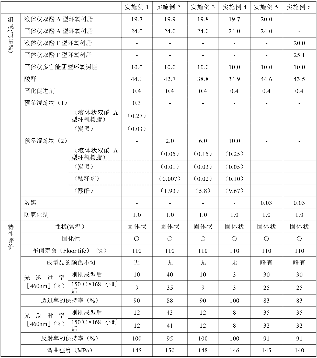
[0061] In order to obtain the compounding amount of the composition shown in Table 1, first, the above-mentioned pre-kneaded product (1), liquid bisphenol A epoxy resin ("YD-8125") at room temperature, bisphenol A type epoxy resin ("YD-8125") solid at room temperature, Phenol A type epoxy resin (produced by Mitsubishi Chemical Co., Ltd., trade name "Epikote 1002" ("Epikote 1002")), a trifunctional epoxy resin with a triazine skeleton in a solid state at room temperature (Nissan Chemical Industry Co., Ltd. ), product name "TEPIC-S"), liquid acid anhydride at room temperature (manufactured by Shin Nippon Chemical Co., Ltd., product name "RIKACID MH-700" ("RIKACID MH-700")), and di Butylated hydroxytoluene (BHT) is mixed at a temperature of 70°C by a universal mixer, and secondly, in the mixture, dimethyl tributylphosphonium phosphate (manufactured by Nippon Chemical Industry Co., Ltd.) is added as a curing accelerator , trade name "ヒシコーリン PX-4MP" ("HISHICOLINPX-4MP")), further k...

Embodiment 2~4

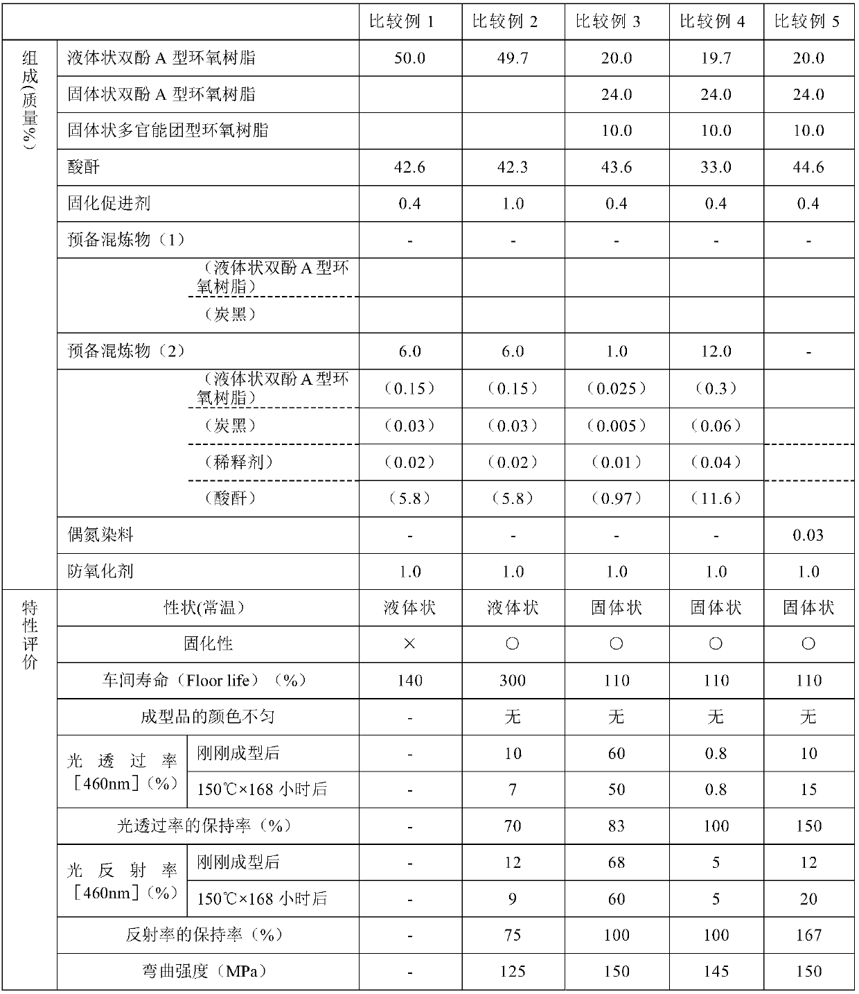
[0062] (Examples 2-4, Comparative Examples 1-4)

[0063] Except that the pre-kneaded product (2) was used instead of the pre-kneaded product (1), and the compounding amount was set so that the compounding amount of each component became the composition shown in Tables 1 and 2, it was the same as in Example 1. operation to obtain a resin composition for optical semiconductors.

Embodiment 5

[0065] Except having mixed carbon black and another component as it was without using the pre-kneaded product, it carried out similarly to Example 1, and obtained the resin composition for optical semiconductors of the composition similar to Example 1.


PUM

PropertyMeasurementUnit
particle diameteraaaaaaaaaa
particle sizeaaaaaaaaaa
particle diameteraaaaaaaaaa

Abstract

A resin composition for an optical semiconductor, a manufacturing method thereof, and an optical semiconductor device for encapsulating a semiconductor element by using the composition, the resin composition for the optical semiconductor being characterized by comprising (A) an epoxy resin containing a solid epoxy resin, (B) a liquid acid anhydride, (C) a curing accelerator and (D) carbon black having an average primary particle diameter of 1 to 50 nm, the content of the (D) carbon black being 0.01-0.05 % by mass of the whole composition.

Description

technical field [0001] This invention relates to the resin composition for optical semiconductors, its manufacturing method, and an optical semiconductor device. Background technique [0002] In optical semiconductor devices (optical devices) incorporating light-emitting elements such as light-emitting diodes and semiconductor lasers, transparent resin compositions with high transmittance have been used as sealing materials for light-emitting elements for the purpose of improving brightness. Generally used methods for sealing include dropping a liquid thermosetting resin under normal pressure or vacuum and pouring it into a box or mold containing parts and curing it (casting method). Methods based on transfer molding, compression molding. In the casting method, a so-called two-component sealing material is used, while in transfer molding and compression molding, a solid sealing material is used. From the viewpoint of productivity, the latter method is preferable. [0003]...

Claims


Application Information

Patent Timeline
Patent Type & Authority Applications(China)
IPC IPC(8): C08L63/00C08K3/04C08K5/13C08K5/521C08G59/42H01L33/56
Inventor 冈本正法
Owner KYOCERA CORP
Why Eureka
Try Eureka