Fingerprint identification sensor, manufacturing method thereof and display device

A fingerprint sensor and fingerprint recognition technology, which is applied in character and pattern recognition, acquisition/organization of fingerprints/palmprints, instruments, etc., can solve problems such as circuit delay, load increase, and influence on manufacturing process, so as to improve deformation and product quality , the effect of reducing stress

Active Publication Date: 2018-02-02
BOE TECH GRP CO LTD
View PDF9 Cites 14 Cited by
  • Summary
  • Abstract
  • Description
  • Claims
  • Application Information

AI Technical Summary

Problems solved by technology

However, the metal light-shielding layer will form a large-area metal area on the surface of the glass substrate. When the display panel is pressed, the metal light-shielding layer will generate greater stress, thereby making the glass substrate easily deformed and affecting the subsequent manufacturing process; the metal light-shielding layer is A large-area metal lay

Method used


Image

  • Fingerprint identification sensor, manufacturing method thereof and display device
  • Fingerprint identification sensor, manufacturing method thereof and display device
  • Fingerprint identification sensor, manufacturing method thereof and display device

Examples


Example Embodiment

[0047] In order to improve the product quality of the display device, embodiments of the present invention provide a fingerprint recognition sensor, a manufacturing method thereof, and a display device. In order to make the objectives, technical solutions, and advantages of the present invention clearer, the following examples are given to further illustrate the present invention in detail.

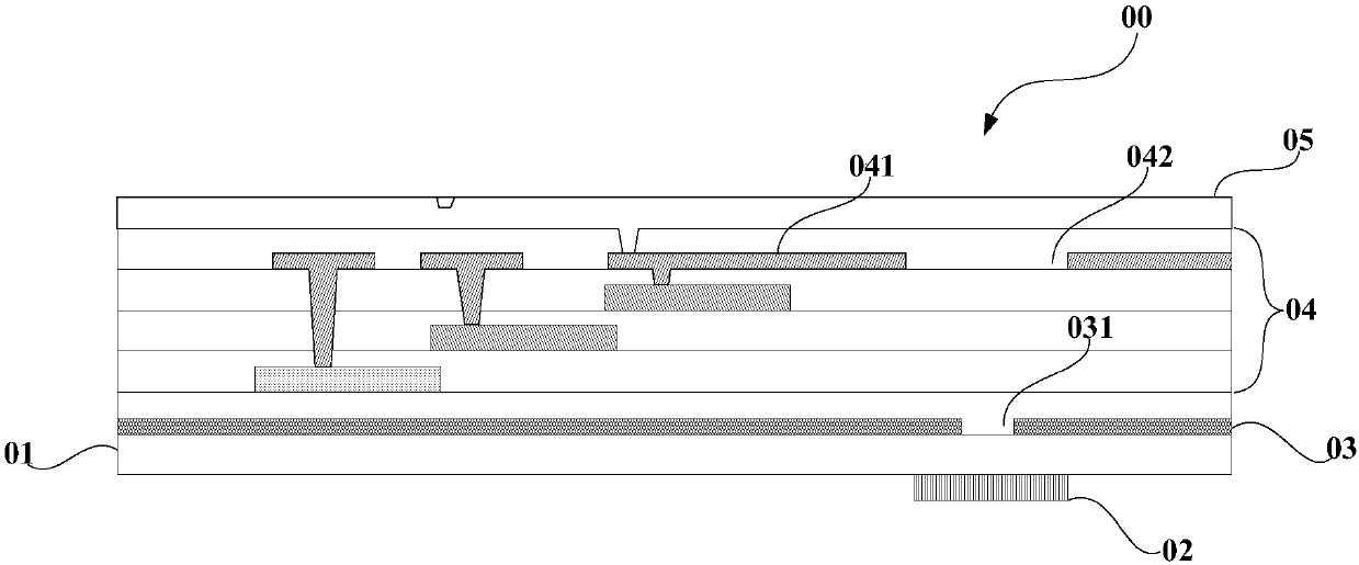
[0048] In related technologies, such as figure 1 As shown, the display panel includes a display area (not shown in the figure) and a fingerprint recognition area 00. The fingerprint recognition area 00 includes a base substrate 01, an image sensor 02 arranged on one side of the base substrate 01, and a metal light-shielding layer 03, a thin film transistor 04 and an OLED device 05 arranged on the other side of the base substrate 01 in sequence, of which: The metal light-shielding layer 03 is arranged close to the base substrate 01 and has an imaging hole 031 opposite to the image sensor 02; ...


PUM

PropertyMeasurementUnit
Diameteraaaaaaaaaa
Diameteraaaaaaaaaa

Abstract

The invention relates to the technical field of fingerprint identification, and discloses a fingerprint identification sensor, a manufacturing method thereof and a display device so as to improve theproduct quality of the display device. The fingerprint identification sensor comprises a plurality of fingerprint identification units arranged in an array mode, and is characterized in that each fingerprint identification unit comprises a substrate base plate, an image acquisition device arranged at one side of the substrate base plate and a first grating structure and a second grating structurewhich are sequentially arranged at the other side of the substrate base plate, the first grating structure is provided with a first imaging hole opposite to image acquisition device in position, the second grating structure is provided with a second imaging hole opposite to the image acquisition device in position, and a slit extending direction of the first grating structure is perpendicular to the a slit extending direction of the second grating structure.

Description

Technical field [0001] The present invention relates to the technical field of fingerprint identification, in particular to a fingerprint identification sensor, a manufacturing method thereof, and a display device. Background technique [0002] With the rapid development of e-commerce and e-banking, people have higher and higher requirements for security. How to accurately identify personal identity and protect information security is a key social problem that must be solved in the current information age. Biometric identification uses the inherent physiological characteristics or behavioral characteristics of the human body to perform personal identification, which has high security and is gradually used in people's daily life. Biometric recognition usually includes face recognition, fingerprint recognition, iris recognition, voice recognition, or hand blood vessel distribution recognition. [0003] OLED (Organic Light-Emitting Diode, Organic Light-Emitting Diode) display device ...

Claims


Application Information

Patent Timeline
IPC IPC(8): G06K9/00
CPCG06V40/1318G02B5/003
Inventor 刘文渠张锋吕志军董立文张世政党宁
Owner BOE TECH GRP CO LTD
Why Eureka
Try Eureka