Vertical memory device and method of manufacturing the same

一种垂直存储、垂直方向的技术,应用在垂直存储器件及其制造领域,能够解决串扰、不稳定、尺寸易变等问题

Active Publication Date: 2018-02-06
SAMSUNG ELECTRONICS CO LTD
View PDF9 Cites 19 Cited by
  • Summary
  • Abstract
  • Description
  • Claims
  • Application Information

AI Technical Summary

Problems solved by technology

Therefore, the trap density in the charge-trapping pattern is insufficient for each cell of the vertical NAND flash memory device, which makes the memory window size of the flash memory device very variable and unstable in response to the size of the flash memory device.
[0006] In addition, the reduction of the vertical gap distance between adjacent stacked cells generally results in electron diffusion and crosstalk between adjacent stacked cells in vertical NAND flash memory devices.

Method used


Image

  • Vertical memory device and method of manufacturing the same
  • Vertical memory device and method of manufacturing the same
  • Vertical memory device and method of manufacturing the same

Examples


Embodiment Construction

[0027] Reference will now be made to some example embodiments illustrated in the drawings, wherein like reference numerals may refer to like parts throughout.

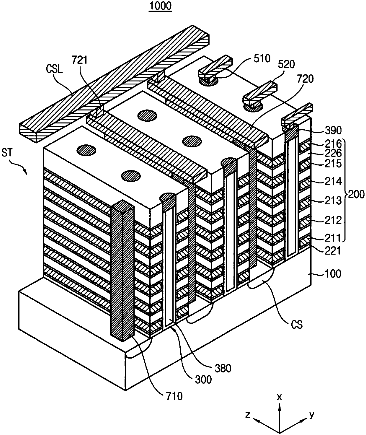
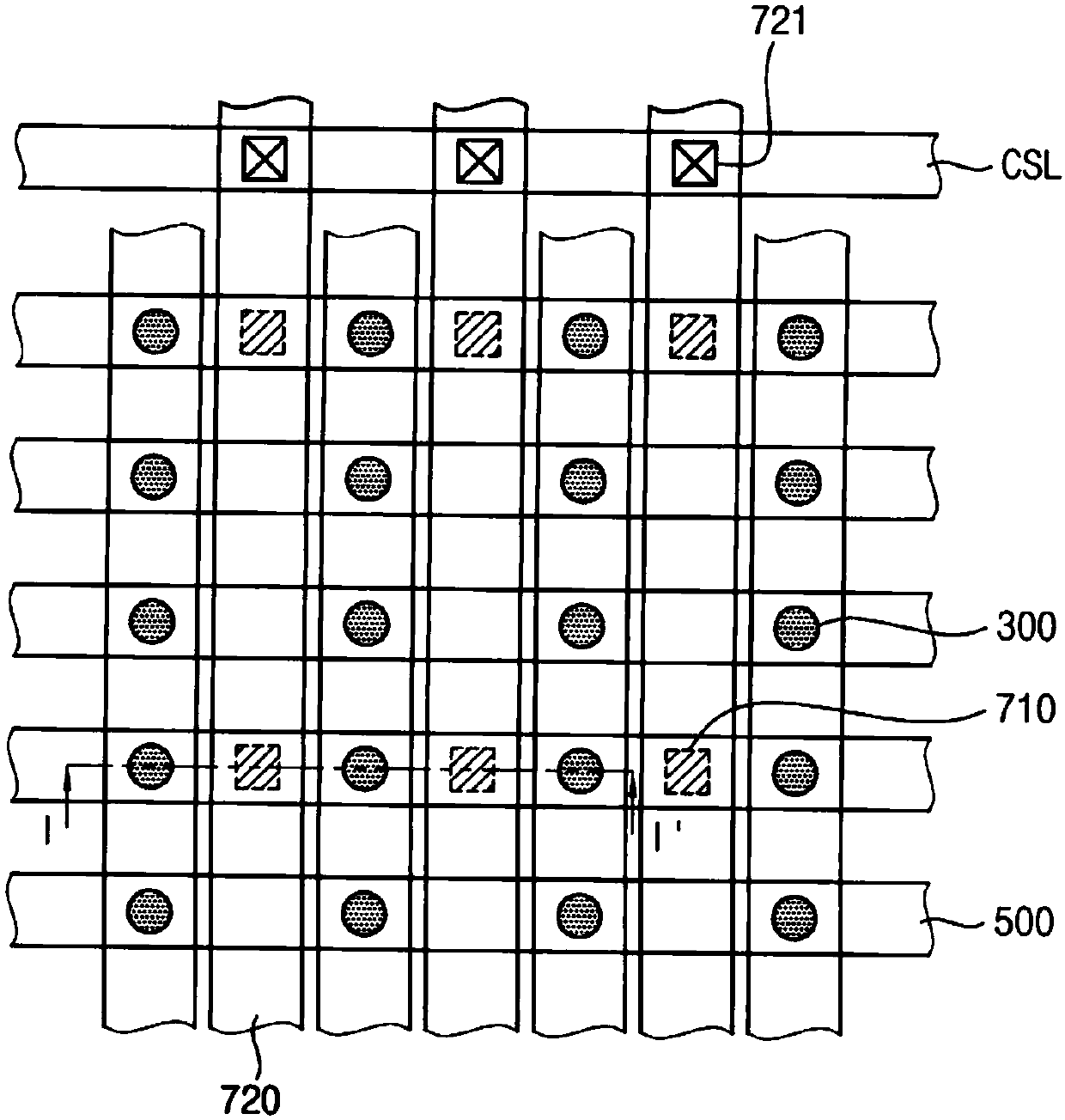
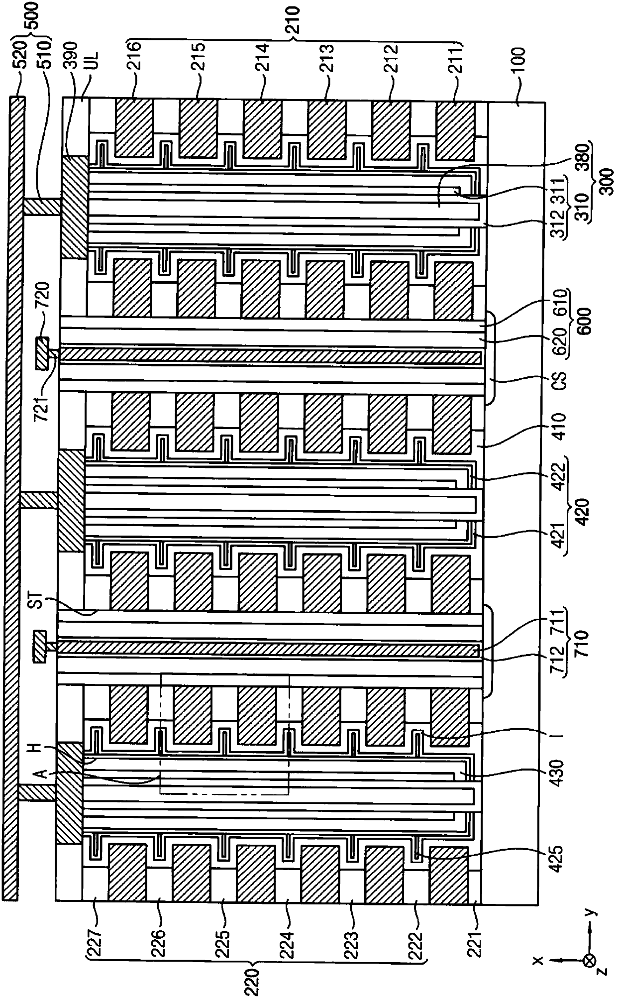
[0028] figure 1 is a perspective view illustrating a vertical nonvolatile memory device according to some example embodiments of the inventive concept, figure 2 is showing figure 1 The top view of the vertical nonvolatile memory device shown in . image 3 is showing figure 1 The vertical nonvolatile memory device shown in the edge figure 2 The cross-sectional view taken along the line I-I'. Figure 4 Yes image 3 Enlarged view of part A of .

[0029] refer to Figures 1 to 4 , The vertical nonvolatile memory device 1000 according to some example embodiments of the inventive concept may include: a gate stack structure 200 having a conductive structure and an insulating interlayer structure alternately stacked in the first direction x on the substrate 100; Active pillar 300, which penetrates the gate stack stru...


PUM


Abstract

Disclosed are vertical memory devices and methods of manufacturing the same. The vertical memory device may include includes a substrate, a gate stack structure and channel structure on the substrate,and a charge trap structure between the gate stack structure and the channel structure. The gate stack structure includes conductive structures and insulation interlayer structures that are alternately stacked on each other in a vertical direction on the substrate such that cell regions and inter-cell regions are alternately arranged in the vertical direction. The channel structure penetrates through the gate stack structure in the vertical direction. The charge trap structure and the conductive structures define memory cells at the cell regions. The charge structure is configured to selectively store charges. The charge trap structure includes an anti-coupling structure in the inter-cell region for reducing a coupling between neighboring memory cells adjacent to each other in the vertical direction.

Description

technical field [0001] Example embodiments relate to vertical memory devices and methods of manufacturing the same, and more particularly, to vertical NAND flash memory devices and / or methods of manufacturing the same. Background technique [0002] In order to increase the storage capacity of NAND memory devices, vertical NAND flash memory devices in which a plurality of memory cells are vertically stacked on a substrate have been proposed. [0003] As vertical NAND flash memory devices tend to be miniaturized coupled with high stacking density of memory cells, electron diffusion and crosstalk occur more frequently between vertically adjacent stacked cells, which affects the reliability of vertical NAND flash memory devices . [0004] In order to reduce and / or minimize electron diffusion and crosstalk between vertically stacked cells, charge-trapping patterns are arranged as individual patterns by each cell in the vertical direction. [0005] As the stacking density of mem...

Claims


Application Information

Patent Timeline
Patent Type & Authority Applications(China)
IPC IPC(8): H01L27/11565H01L27/11568H01L27/11578
CPCH10B43/30H10B43/10H10B43/20H10B43/35H10B43/27H01L29/7926H10B43/23
Inventor 金森宏治殷东锡
Owner SAMSUNG ELECTRONICS CO LTD
Why Eureka
Try Eureka