Fingerprint recognition module structure, manufacturing method and terminal equipment
A fingerprint recognition module and fingerprint recognition technology, which are used in character and pattern recognition, acquisition/organization of fingerprints/palmprints, semiconductor/solid-state device manufacturing, etc. , reduce the unlocking success rate and other issues, to achieve the effect of improving imaging quality, increasing the screen area ratio, increasing the unlocking success rate and screen area ratio
- Summary
- Abstract
- Description
- Claims
- Application Information
AI Technical Summary
Problems solved by technology
Method used
Image

Examples
Embodiment 1
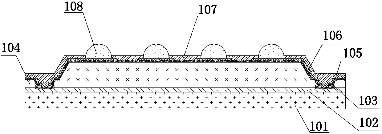
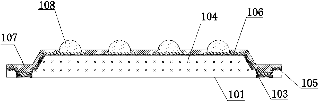
[0040] Figure 1A A schematic diagram of the structure of a fingerprint identification chip provided by Embodiment 1 of the present invention; Figure 1B A schematic diagram of another fingerprint identification chip structure provided by Embodiment 1 of the present invention; Figure 1C A schematic diagram of the structure of a fingerprint identification module provided by Embodiment 1 of the present invention; Figure 1D It is a schematic diagram of another fingerprint recognition module structure provided by Embodiment 1 of the present invention. The fingerprint recognition module in the embodiment of the present invention is preferably a fingerprint recognition module in a full-screen mobile phone, and this technical solution can also be applied to a display screen of an electronic device such as a tablet or a computer.
[0041] Such as Figure 1A As shown, the fingerprint recognition chip structure includes a fingerprint recognition chip 104 , a filter layer 101 and a pa...
Embodiment 2
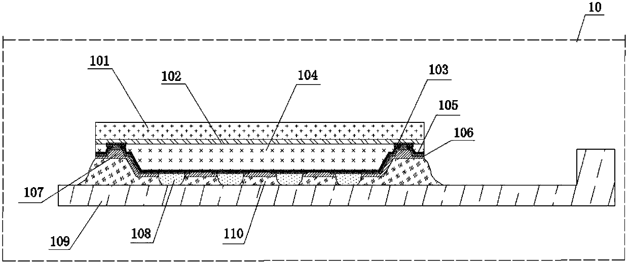
[0057] Figure 2A It is a top structural block diagram of a terminal device provided in Embodiment 2 of the present invention. Figure 2B It is a schematic cross-sectional structural diagram of a terminal device provided by Embodiment 2 of the present invention. Figure 2C It is a schematic cross-sectional structural diagram of another terminal device provided in Embodiment 2 of the present invention. Such as Figure 2A As shown, the terminal device 20 includes the fingerprint recognition module structure 10 provided in Embodiment 1 of the present invention.
[0058] Wherein, the terminal device 20 may be an electronic terminal device such as a mobile phone, a tablet, or a computer that can have a fingerprint recognition function.
[0059] Optionally, the terminal device 20 further includes a display screen 30 , and the fingerprint identification module 10 is attached below the display screen 30 .
[0060] Exemplarily, the embodiment of the present invention is described b...
Embodiment 3
[0064] image 3 It is a schematic flowchart of a manufacturing method of a fingerprint recognition module structure provided by Embodiment 3 of the present invention. Figures 4A-4O It is a schematic diagram of a process flow of a manufacturing method of a fingerprint recognition module structure provided by Embodiment 3 of the present invention. This method can be used to prepare any fingerprint identification module structure provided in the above embodiments. It should be noted that the manufacturing method of the fingerprint identification module structure in the embodiment of the present invention is to prepare on the fingerprint wafer, and after the fingerprint identification chip structure is manufactured, it is divided into individual chips and bonded to the flexible circuit board. . The drawings provided in the embodiments of the present invention use a single fingerprint identification chip as an illustration, but in the manufacturing process, the entire fingerprin...
PUM
 Abstract
Description
Claims
Application Information
 - R&D
- Intellectual Property
- Life Sciences
- Materials
- Tech Scout
- Unparalleled Data Quality
- Higher Quality Content
- 60% Fewer Hallucinations
Browse by: Latest US Patents, China's latest patents, Technical Efficacy Thesaurus, Application Domain, Technology Topic, Popular Technical Reports.
© 2025 PatSnap. All rights reserved.Legal|Privacy policy|Modern Slavery Act Transparency Statement|Sitemap|About US| Contact US: help@patsnap.com