AI technical title is built by Patsnap AI team. It summarizes the technical point description of the patent document.
A three-level inverter and capacitor technology, applied in electrical components, high-efficiency power electronic conversion, conversion of AC power input to DC power output, etc., can solve problems such as large circuit conduction losses
Inactive Publication Date: 2018-02-09
EMERSON NETWORK POWER CO LTD
View PDF3 Cites 0 Cited by
Summary
Abstract
Description
Claims
Application Information
AI Technical Summary
This helps you quickly interpret patents by identifying the three key elements:
Problems solved by technology
Method used
Benefits of technology
Problems solved by technology
[0006] The embodiment of the present application provides a three-level inverter to solve the problem of large circuit conduction loss in the prior art
Method used
Image
Click on the blue label to locate the original text in one second.
Reading with bidirectional positioning of images and text.
Examples
Embodiment 1
[0022] Embodiment 1 of the present application provides a three-level inverter, such as Figure 4 As shown, it may include a first transistor Q1, a second transistor Q2, a first capacitor C1, a second capacitor C2, a third transistor Q3 and a fourth transistor Q4, wherein:
[0023] The collector of the first transistor Q1 is connected to the positive bus terminal Vbus1 of the three-level inverter; the emitter of the second transistor Q2 is connected to the negative bus terminal Vbus2 of the three-level inverter;
[0024] When the conduction time of the first transistor Q1 is greater than or equal to 1 / N period, the first transistor Q1 adopts a transistor with optimized conduction loss, and the second transistor Q2 adopts a transistor with optimized switching loss;
[0025] When the conduction time of the second transistor Q2 is greater than or equal to 1 / N period, the second transistor Q2 adopts a transistor with optimized conduction loss, and the first transistor Q1 adopts a ...
Embodiment 2
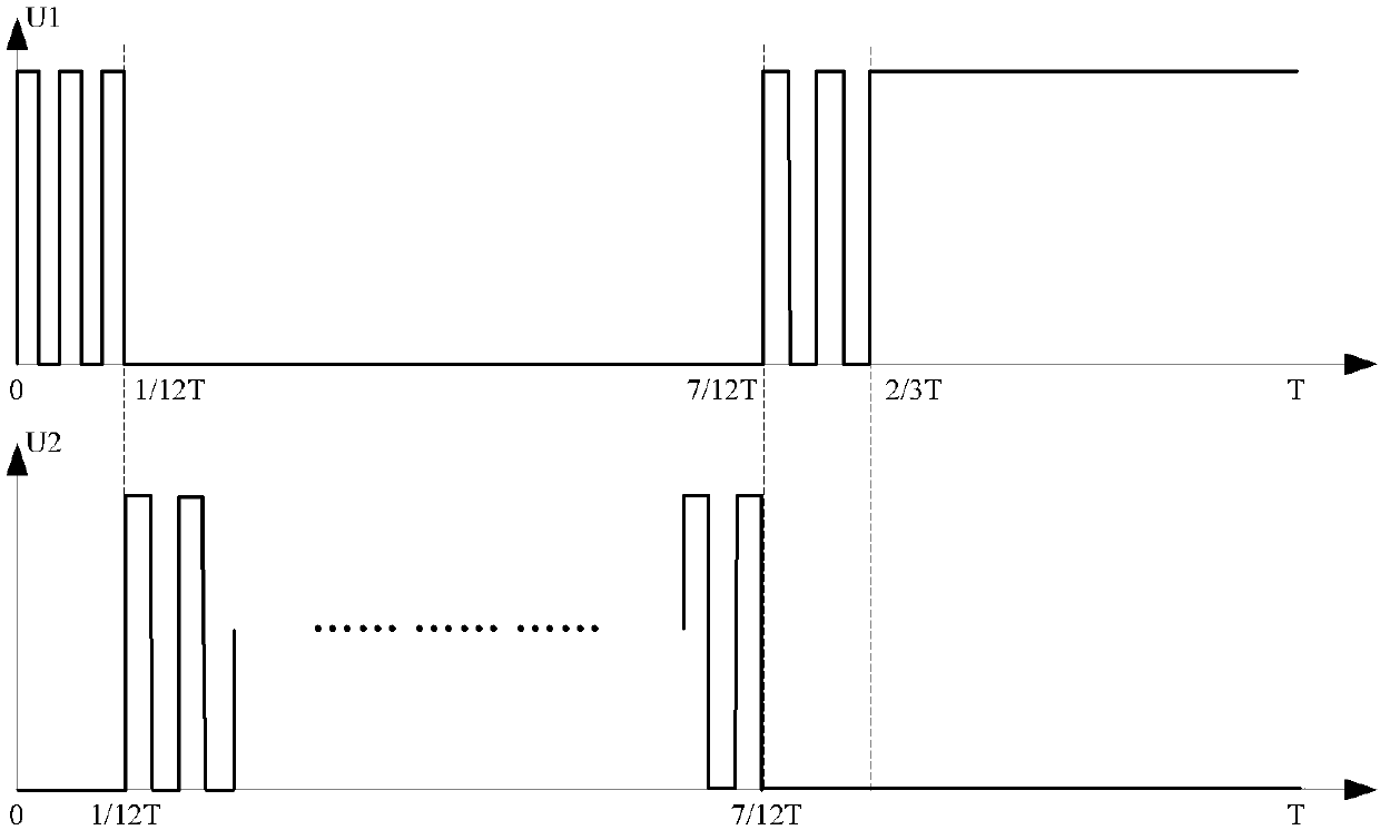
[0043] Embodiment 2 of the present application provides a three-level inverter, such as Figure 5 As shown, it may include a first transistor D1, a second transistor D2, a first capacitor C1, a second capacitor C2, a fifth transistor, a sixth transistor, a first diode and a second diode, wherein:
[0044] The collector of the first transistor Q1 is connected to the positive bus terminal Vbus1 of the three-level inverter; the emitter of the second transistor Q2 is connected to the negative bus terminal Vbus2 of the three-level inverter;
[0045] When the conduction time of the first transistor Q1 is greater than or equal to 1 / N period, the first transistor Q1 adopts a transistor with optimized conduction loss, and the second transistor Q2 adopts a transistor with optimized switching loss;
[0046] When the conduction time of the second transistor Q2 is greater than or equal to 1 / N period, the second transistor Q2 adopts a transistor with optimized conduction loss, and the first...
PUM
Abstract
The invention discloses a three-level inverter with little circuit conduction loss. The three-level inverter comprises a first transistor and a second transistor, wherein the collector of the first transistor is connected with the positive bus end of the three-level inverter; the emitter of the second transistor is connected with the negative bus end of the three-level inverter; when the conduction time of the first transistor is greater than or equal to a 1 / N period, the first transistor adopts a transistor which optimizes the conduction loss, and the second transistor adopts a transistor which optimizes switch loss; and when the conduction time of the second transistor is greater than or equal to the 1 / N period, the second transistor adopts a transistor which optimizes the conduction loss, and the first transistor adopts a transistor which optimizes the switch loss, and N is a preset real number larger than 1.
Description
technical field [0001] The present application relates to the technical field of electronic circuits, in particular to a three-level inverter. Background technique [0002] In the prior art three-level inverter, the main functional devices include four transistors, wherein: the collector of the first transistor is connected to the positive bus terminal, and the emitter of the second transistor is connected to the negative bus segment; the first transistor and The second transistor uses the same type of transistor, and the third transistor and the fourth transistor use the same type of transistor. [0003] The above-mentioned three-level inverter implements inverter control by inputting different modulation pulses to the base of each transistor, so as to convert the DC power input from the positive bus terminal and the negative bus terminal into AC power and output it from the AC output terminal. In the prior art, Space VectorPulse Width Modulation (SVPWM) control is usuall...
Claims
Application Information
Patent Timeline
Application Date:The date an application was filed.
Publication Date:The date a patent or application was officially published.
First Publication Date:The earliest publication date of a patent with the same application number.
Issue Date:Publication date of the patent grant document.
PCT Entry Date:The Entry date of PCT National Phase.
Estimated Expiry Date:The statutory expiry date of a patent right according to the Patent Law, and it is the longest term of protection that the patent right can achieve without the termination of the patent right due to other reasons(Term extension factor has been taken into account ).
Invalid Date:Actual expiry date is based on effective date or publication date of legal transaction data of invalid patent.

