Carrier storage type FS-IGBT with low conduction voltage drop and manufacturing method thereof

A carrier storage and low conduction technology, applied in the field of microelectronics, can solve problems such as limiting IGBT performance, and achieve the effects of reducing switching loss, reducing feedback capacitance, and reducing conduction voltage drop

Pending Publication Date: 2021-05-04
WUXI TONGFANG MICROELECTRONICS
View PDF0 Cites 0 Cited by
  • Summary
  • Abstract
  • Description
  • Claims
  • Application Information

AI Technical Summary

Problems solved by technology

As the size of semiconductor wafers continues to increase, cost, process complexity, and fragmentation rate limit the continuous improvement of IGBT (especially low-voltage IGBT) performance

Method used


Image

  • Carrier storage type FS-IGBT with low conduction voltage drop and manufacturing method thereof
  • Carrier storage type FS-IGBT with low conduction voltage drop and manufacturing method thereof

Examples


Embodiment Construction

[0025]The present invention is further explained in conjunction with specific embodiments.

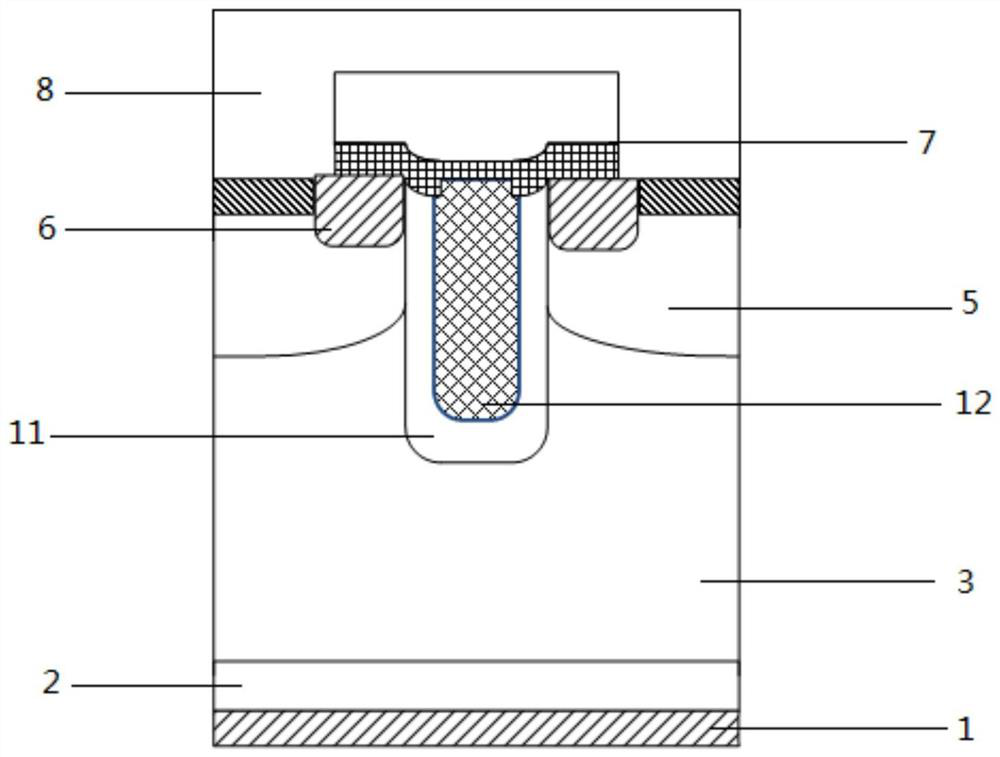
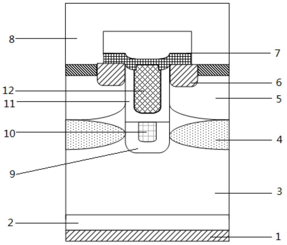
[0026]A carrier storage type FS-IGBT of a low-conducting passage, which includes a P + type collector 1, N + type buffer layer 2, N-substrate 3, N + type carrier storage layer 4, P-type The body region 5, the N + -type emitter 6, the insulative dielectric layer 7, the emitter metal 8, the shield gate oxide layer 9, the shielding gate polysilicon 10, the gate oxide layer 11 and the gate conductive polysilicon 12;

[0027]The groove is opened downward on the front side of the N-substrate 3, and the shield gate oxide layer 9 is disposed on the lower side of the trench, and the shield gate polysilicon 10 is provided in the shielding gate oxide layer 9, and the upper side of the groove and the upper side of the trench and The gate oxide layer 11 is provided on the shield gate polysilicon 10, and a gate conductive polysilicon 12 is provided in the gate oxide layer 11;

[0028]The front side of the N-substr...


PUM


Abstract

The invention relates to a carrier storage type FS-IGBT with low conduction voltage drop. The carrier storage type FS-IGBT is characterized in that: a trench is formed in an N-type substrate, and a shield gate oxide layer, shield gate polycrystalline silicon, a gate oxide layer and gate conductive polycrystalline silicon are arranged in the trench; an N+ type carrier storage layer is formed on the front surface of the N- type substrate, a P- type body region is formed on the front surface of the N+ type carrier storage layer, an N+ type emitter is formed on the front surface of the P-type body region, an insulating dielectric layer is arranged on the front surface of the N+ type emitter, and emitter metal is arranged on the front surface of the insulating dielectric layer; and an N+ type buffer layer is arranged on the back face of the N- type substrate, and a P+ type collector is arranged on the back face of the N+ type buffer layer. According to the carrier storage type FS-IGBT, the conduction voltage drop is reduced, the feedback capacitance is reduced, the conduction loss of the device during working is improved, and finally the switching loss is reduced to a certain extent.

Description

Technical field[0001]The present invention belongs to the field of microelectronics, and is specifically a carrier storage type FS-IGBT and manufacturing method of low-conducting pressure drop.Background technique[0002]Compared to MOSFETs, the electrical conductive modulation effect of the substrate of the IGBT device can greatly reduce the forward travel pressure drop, the static power loss is small, the higher the voltage, and the performance is more significant. Thus, IGBT accounts great market share in medium and high pressure applications. IGBT mainly has three structures of PT-IGBT, non-pendant NPT-IGBT and field cutoff FS-IGBT, and the main differences between the three are different substrate PN junction structures and different substrate thicknesses. For PT-IGBT and NPT-IGBT, the FS-IGBT has the thinnest thickness, and its forward conduction is significantly decreased, and the structure has been widely used in IGBT products. As the semiconductor wafer is continuously improv...

Claims


Application Information

Patent Timeline
Patent Type & Authority Applications(China)
IPC IPC(8): H01L29/06H01L29/423H01L29/739H01L21/28H01L21/331
CPCH01L29/0684H01L29/401H01L29/42356H01L29/66348H01L29/7397H01L29/7398
Inventor 史志扬张海涛
Owner WUXI TONGFANG MICROELECTRONICS
Why Eureka
Try Eureka