

Array substrate and method of manufacturing the same, and display panel
A technology for array substrates and substrates, which can be applied to electrical components, electrical solid-state devices, circuits, etc., and can solve problems such as uneven film layers.
- Summary
- Abstract
- Description
- Claims
- Application Information
AI Technical Summary
Problems solved by technology
Method used
Image

Examples
Embodiment 1
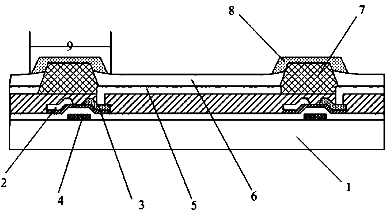
[0035] see figure 1 , which shows a structural block diagram of an array substrate according to Embodiment 1 of the present invention, specifically including:
[0036] The substrate 1 is then patterned to form an anode layer 5 and a first pixel defining layer 7 on the substrate 1, the light emitting layer 6 covering the anode layer 5, and the first pixel defining layer 7 formed on the first pixel defining layer 7 Two pixel defining layers 8, the second pixel defining layer 8 covers the edge region 9 of the light emitting layer.
[0037] In practical applications, the substrate 1 may be a substrate on which a thin film transistor array has been fabricated, or other substrates, which are not specifically limited in the present invention. The thin film transistor includes a source 2 , a drain 3 and a gate 4 .
[0038] The first pixel defining layer 7 has a regular trapezoidal structure, and the orthographic projection of the upper cross section of the first pixel defining layer ...
Embodiment 2
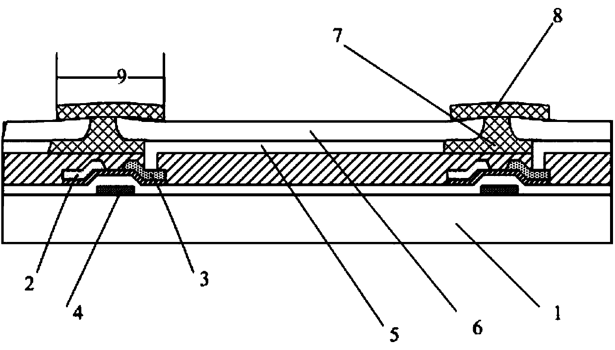
[0047] see figure 2 , which shows a structural block diagram of an array substrate described in Embodiment 2 of the present invention. The array substrate is basically the same as the array substrate described in Embodiment 1. For the same parts, you can refer to the content in Embodiment 1. This embodiment The second example mainly illustrates the differences from the first embodiment, which mainly lies in the different structures of the first pixel defining layer 7 and the second pixel defining layer 8 .
[0048] In the second embodiment, the first pixel defining layer has a tapered structure on the substrate. The tapered structure refers to the way in which the cross section of the first pixel defining layer decreases gradually on the substrate. The tapered structure specifically includes : the first pixel defining layer 7 adopts a structure with a narrow top and a wide bottom, that is, the first pixel defining layer 7 includes a first part close to the substrate and a sec...
Embodiment 3
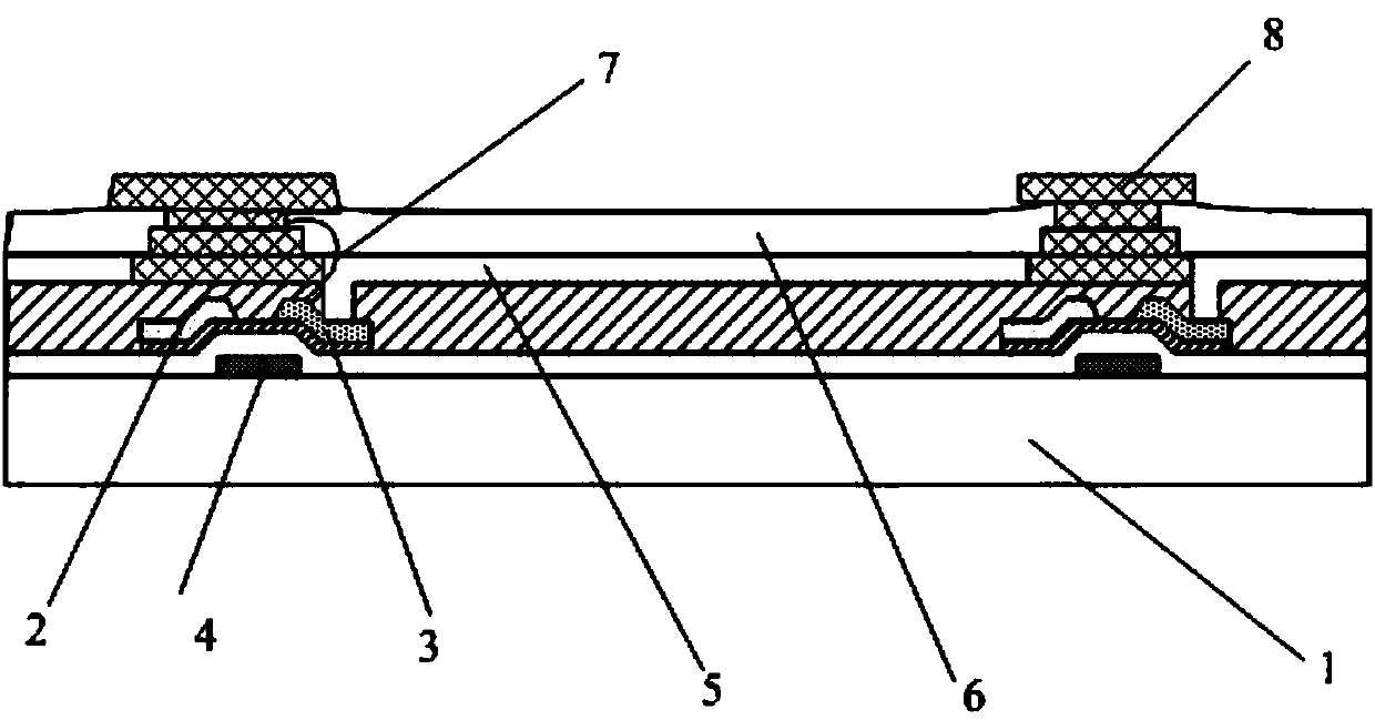
[0052] see image 3 , which shows a structural block diagram of an array substrate described in Embodiment 3 of the present invention. The array substrate is basically the same as the array substrate described in Embodiment 1. For the same parts, you can refer to the content in Embodiment 1. The main differences are The difference is that the structures of the first pixel defining layer and the second pixel defining layer are different,
[0053] In the third embodiment, the first pixel defining layer has a tapered structure on the substrate. The tapered structure means that the cross-section of the first pixel defining layer decreases gradually on the substrate. The tapered structure specifically includes : what the first pixel defining layer 7 adopts is a ladder structure, and there are at least two steps or more steps in the ladder structure, the present invention does not specifically limit this, and the light emission can be reduced by setting the first pixel defining laye...
PUM
 Abstract
Description
Claims
Application Information