Heterojunction bipolar transistor

A heterojunction bipolar and transistor technology, applied in the direction of semiconductor devices, electrical components, circuits, etc., can solve the problems of lack of control stability, complicated doping process, and reduced yield, so as to reduce the dependence of collector voltage Effect

Active Publication Date: 2018-02-16
MURATA MFG CO LTD
View PDF5 Cites 2 Cited by
  • Summary
  • Abstract
  • Description
  • Claims
  • Application Information

AI Technical Summary

Problems solved by technology

[0004] In the HBT disclosed in Patent Document 1, since the collector layer is formed according to a complex doping profile, the doping process at the time of manufacturing the collector layer becomes complicated, resulting in a lack of control stability and a decrease in yield in mass production. The problem

Method used


Image

  • Heterojunction bipolar transistor
  • Heterojunction bipolar transistor
  • Heterojunction bipolar transistor

Examples


Embodiment Construction

[0045] Hereinafter, embodiments of the present invention will be described in detail with reference to the drawings. In addition, the same code|symbol is attached|subjected to the same element, and repeated description is abbreviate|omitted.

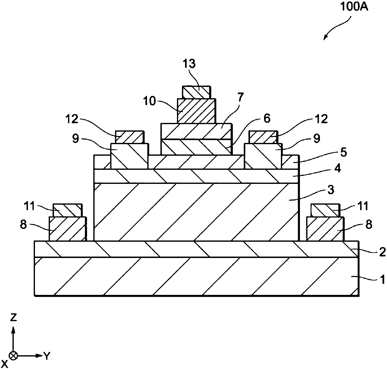
[0046] First, refer to Figure 1 ~ Figure 5B , the HBT according to the first embodiment of the present invention will be described. figure 1 It is a cross-sectional view of HBT100A according to the first embodiment of the present invention. HBT100A is formed on a semiconductor substrate 1 and includes a sub-collector layer 2 , a collector layer 3 , a base layer 4 , an emitter layer 5 , contact layers 6 and 7 , electrodes, wiring, and the like.

[0047] The semiconductor substrate 1 is made of, for example, GaAs, and has a width direction parallel to the Y axis, a depth direction parallel to the X axis, and a thickness direction parallel to the Z axis. Furthermore, the semiconductor substrate 1 has a first principal surface (side in t...


PUM


Abstract

The present invention provides a heterojunction bipolar transistor that combines stable control of its fabrication and a low collector-voltage dependence of base-collector capacitance. An HBT includesa semiconductor substrate having first and second principal surfaces opposite each other; and a collector layer, a base layer, and an emitter layer stacked in this order on the first principal surface side of the semiconductor substrate. The collector layer includes a first semiconductor layer with metal particles dispersed therein, the metal particles each formed by a plurality of metal atoms bonded with each other.

Description

technical field [0001] The present invention relates to heterojunction bipolar transistors. Background technique [0002] In mobile communication devices such as mobile phones, heterojunction bipolar transistors (HBT: Heterojunction Bipolar Transistor) are widely used in order to amplify the power of radio frequency (RF: Radio Frequency) signals transmitted to base stations. In the HBT, when a high-frequency RF signal is amplified, the capacitance between the base and the collector fluctuates according to the fluctuation of the collector voltage, and the distortion characteristic may deteriorate. Therefore, in order to improve the distortion characteristics, it is required that the variation of the base-collector capacitance be small with respect to the variation of the collector voltage (that is, the dependence of the base-collector capacitance on the collector voltage is low). For example, Patent Document 1 discloses an HBT that reduces the collector voltage dependence of...

Claims


Application Information

Patent Timeline
IPC IPC(8): H01L29/737H01L29/08
CPCH01L29/0821H01L29/401H01L29/737H01L29/20H01L29/41708H01L29/66318H01L29/7371H01L29/0817H01L29/12H01L29/66242
Inventor 大部功梅本康成吉田茂柴田雅博
Owner MURATA MFG CO LTD
Why Eureka
Try Eureka