Supercharge Your Innovation With Domain-Expert AI Agents!

Formation method of semiconductor structure

A semiconductor and fin technology, applied in the field of semiconductor structure formation, can solve problems such as poor performance, and achieve the effect of improving interface performance and performance

Active Publication Date: 2021-05-04
SEMICON MFG INT (SHANGHAI) CORP +1
View PDF9 Cites 0 Cited by
  • Summary
  • Abstract
  • Description
  • Claims
  • Application Information

AI Technical Summary

Problems solved by technology

However, core devices that introduce high-K metal gate transistors often have poor performance.

Method used


Image

  • Formation method of semiconductor structure
  • Formation method of semiconductor structure
  • Formation method of semiconductor structure

Examples


Embodiment Construction

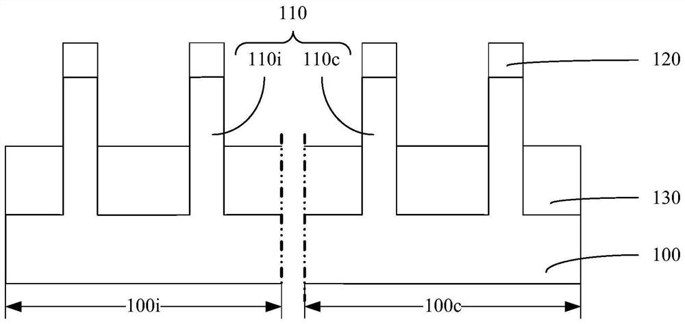
[0028] It can be seen from the background art that the core devices that introduce high-K metal gate transistors often have the problem of poor performance. The reason for the performance problem is now analyzed in combination with the structure of the semiconductor structure in the prior art.

[0029] Since the operating voltages of the core device and the input and output devices are different, the thicknesses of the gate dielectric layers of the core device and the input and output devices are different. Specifically, the thickness of the dielectric layer of the core device is usually smaller than the thickness of the dielectric layer of the input and output devices.

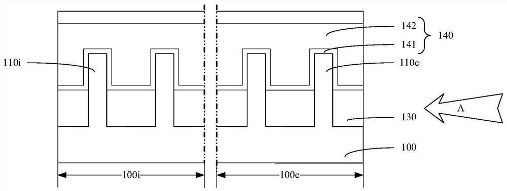
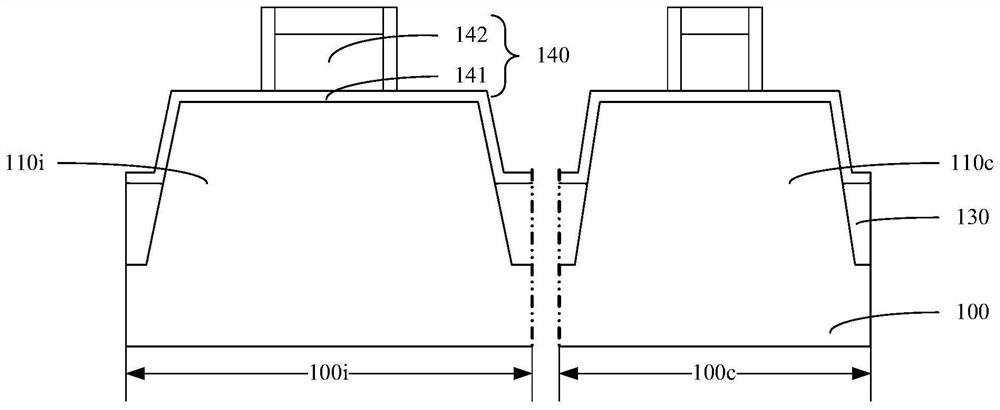
[0030] In the prior art, usually after the fins are formed, an oxide layer is formed on the surface of the fins by thermal oxidation, and a dummy gate is formed on the oxide layer, the dummy gate and the oxide layer constitute a dummy gate structure. After the source region and the drain region are formed, ...


PUM


Abstract

A method for forming a semiconductor structure, comprising: forming a substrate; forming a dummy gate structure; filling a dielectric layer; forming an implant opening; implanting repair ions; removing an oxide layer at the bottom of the implant opening; ; Carry out repairing treatment, so that the repairing ions repair the interface between the fins in the core area and the interface layer. In the present invention, after the implantation opening is formed by forming the dummy gate without the dummy gate structure in the core area, repairing ions are implanted into the core area fin below the oxide layer at the bottom of the implantation opening; then the interface layer is reshaped, and the repairing ions are made Repair the interface between the fins in the core area and the interface layer. The repairing ions can saturate the dangling bonds on the surface of the fin, thereby improving the performance of the interface between the fin in the core region and the interface layer, thereby improving the performance of the formed semiconductor structure.

Description

technical field [0001] The invention relates to the field of semiconductor manufacturing, in particular to a method for forming a semiconductor structure. Background technique [0002] Semiconductor devices are mainly divided into core (Core) devices and input and output (Input and Output, IO) devices according to their functions. Wherein, the core device includes a core MOS device, and the input-output device includes an input-output MOS device. In order to reduce the size of the semiconductor device and improve the integration of the semiconductor device, the size of the core device is smaller than the size of the input and output devices. In addition, the operating voltage of the input and output devices is much higher than that of the core device to obtain stronger driving capability. In order to prevent problems such as electrical breakdown, when the operating voltage of the device is greater, the thickness of the gate dielectric layer of the device is required to be ...

Claims


Application Information

Patent Timeline
Patent Type & Authority Patents(China)
IPC IPC(8): H01L21/336H01L29/423H01L29/78
CPCH01L29/4232H01L29/66795H01L29/785
Inventor 周飞
Owner SEMICON MFG INT (SHANGHAI) CORP
Features
  • R&D
  • Intellectual Property
  • Life Sciences
  • Materials
  • Tech Scout
  • Unparalleled Data Quality
  • Higher Quality Content
  • 60% Fewer Hallucinations
Learn More