
Semiconductor device and manufacturing method thereof

A semiconductor and conductive gate technology, applied in the field of semiconductor devices and their manufacturing, can solve problems such as reducing the full well electron capacity of an image sensor, and achieve the effects of improving image quality, reducing crosstalk, and suppressing dark current

Inactive Publication Date: 2018-03-02
HUAIAN IMAGING DEVICE MFGR CORP
View PDF4 Cites 5 Cited by
  • Summary
  • Abstract
  • Description
  • Claims
  • Application Information

AI Technical Summary

Problems solved by technology

But this method will reduce the full well electronic capacity of the image sensor (Full Well Capacity)

Method used


Image

  • Semiconductor device and manufacturing method thereof
  • Semiconductor device and manufacturing method thereof
  • Semiconductor device and manufacturing method thereof

Examples


Embodiment Construction

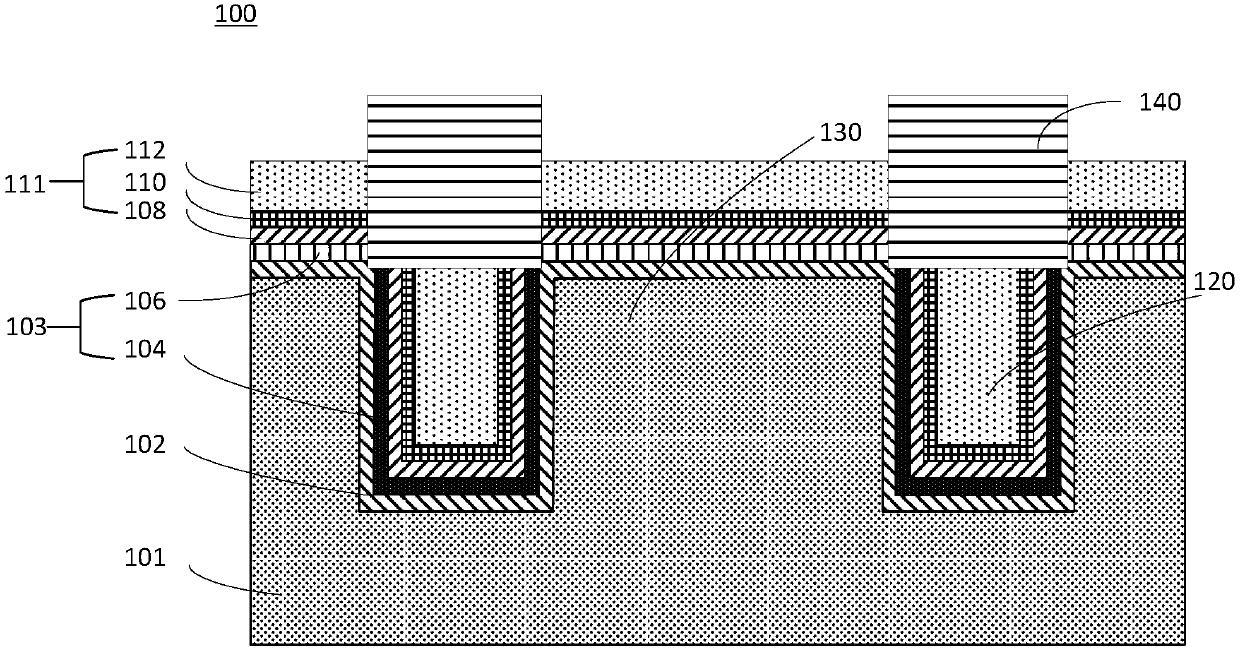
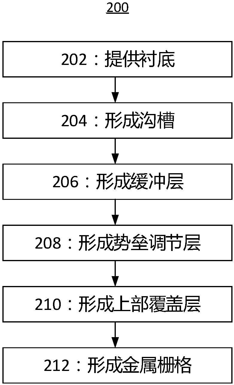
[0040] Various exemplary embodiments of the present disclosure will now be described in detail with reference to the accompanying drawings. It should be noted that the relative arrangements of components and steps, numerical expressions and numerical values ​​set forth in these embodiments do not limit the scope of the present disclosure unless specifically stated otherwise. In addition, techniques, methods, and devices known to persons of ordinary skill in the related art may not be discussed in detail, but where appropriate, such techniques, methods, and devices should be considered part of the authorized specification.

[0041]In the specification and claims, the words "front", "rear", "top", "bottom", "above", "under", etc., if present, are used for descriptive purposes and not necessarily to describe a constant relative position. It is to be understood that the terms so used are interchangeable under appropriate circumstances such that the embodiments of the disclosure d...


PUM


Abstract

The invention relates to a semiconductor device and a manufacturing method thereof. The characteristics lie in that the semiconductor device comprises a substrate, an insulating buffer layer and a barrier adjusting layer, and is characterized in that the substrate comprises trenches and a transmission region separated by the trenches; the insulating buffer layer is formed on the substrate and covers the surfaces of trenches and the transmission region; and the barrier adjusting layer is formed on the buffer layer and used for adjusting barriers at the surface of the substrate, the barrier adjusting layer comprises a first portion which is located on the buffer layer in each trench and a second portion which is located on the buffer layer in the transmission region, the first portion is formed by a conductive material, and the second portion is formed by an insulating material.

Description

technical field [0001] The present disclosure relates to the field of semiconductors, and in particular, to semiconductor devices and methods of manufacturing the same. Background technique [0002] Image sensors may be used to sense radiation (eg, optical radiation, including but not limited to visible light, infrared, ultraviolet, etc.) to generate corresponding electrical signals (images). It is widely used in digital cameras, security devices, and other imaging equipment. Image sensors can be classified into back-illuminated (BSI) image sensors and front-illuminated (FSI) image sensors according to the way they receive radiation. [0003] A backside illuminated (BSI) image sensor is capable of receiving radiation from its backside. Different from front-illuminated (FSI) image sensors, in back-illuminated (BSI) image sensors, radiation is incident from the back of the substrate, while wiring and other components that may affect radiation reception are basically located ...

Claims


Application Information

Patent Timeline
Patent Type & Authority Applications(China)
IPC IPC(8): H01L27/146
Inventor 陈世杰夏绍曾黄晓橹
Owner HUAIAN IMAGING DEVICE MFGR CORP
Learn More