

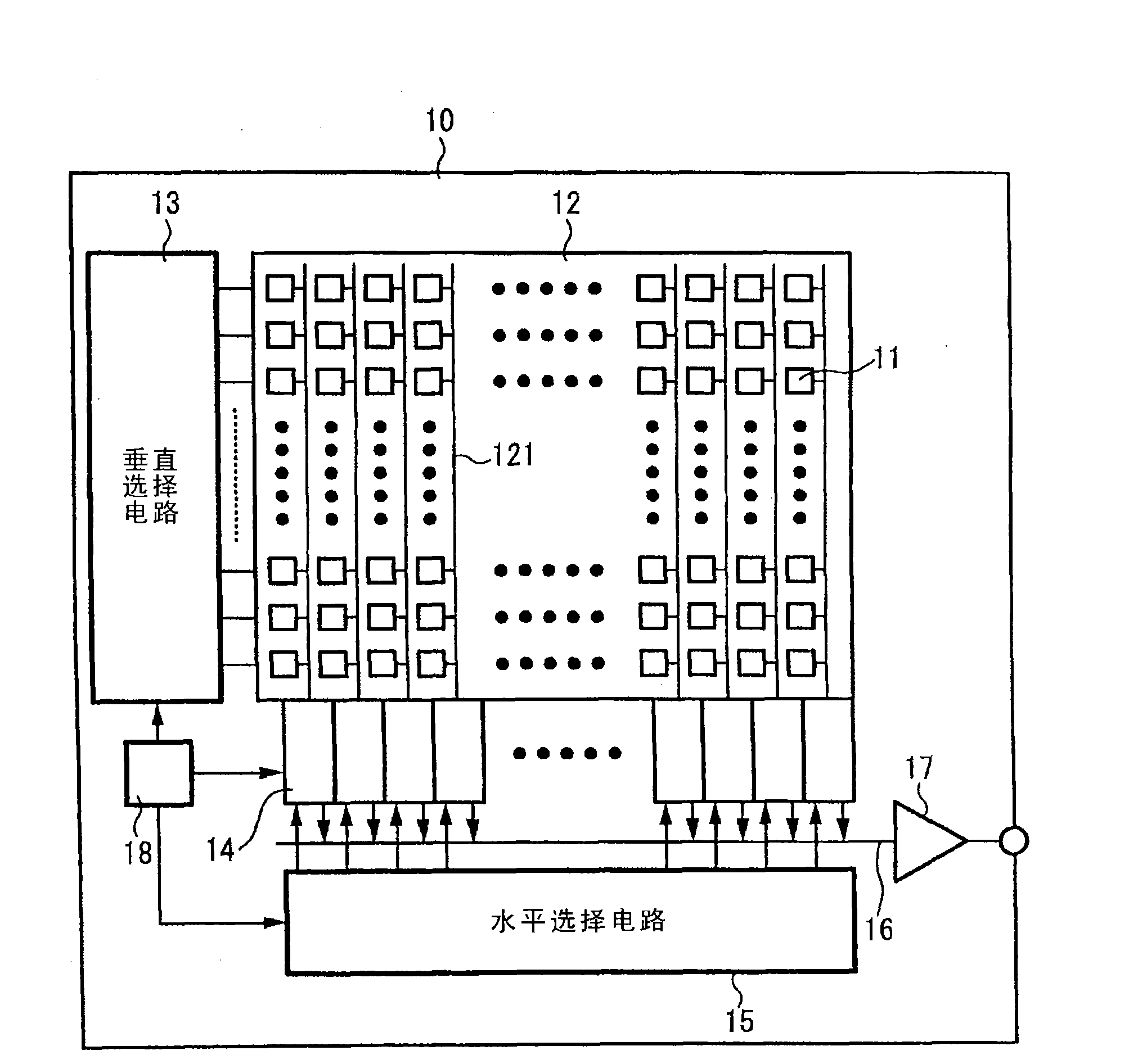
Solid-state imaging device and camera
一种固态成像器件、像素的技术,应用在电固体器件、半导体器件、电气元件等方向,达到电容减小、转换效率增大、提高灵敏度的效果
- Summary
- Abstract
- Description
- Claims
- Application Information
AI Technical Summary
Problems solved by technology
Method used
Image

Examples
Embodiment Construction
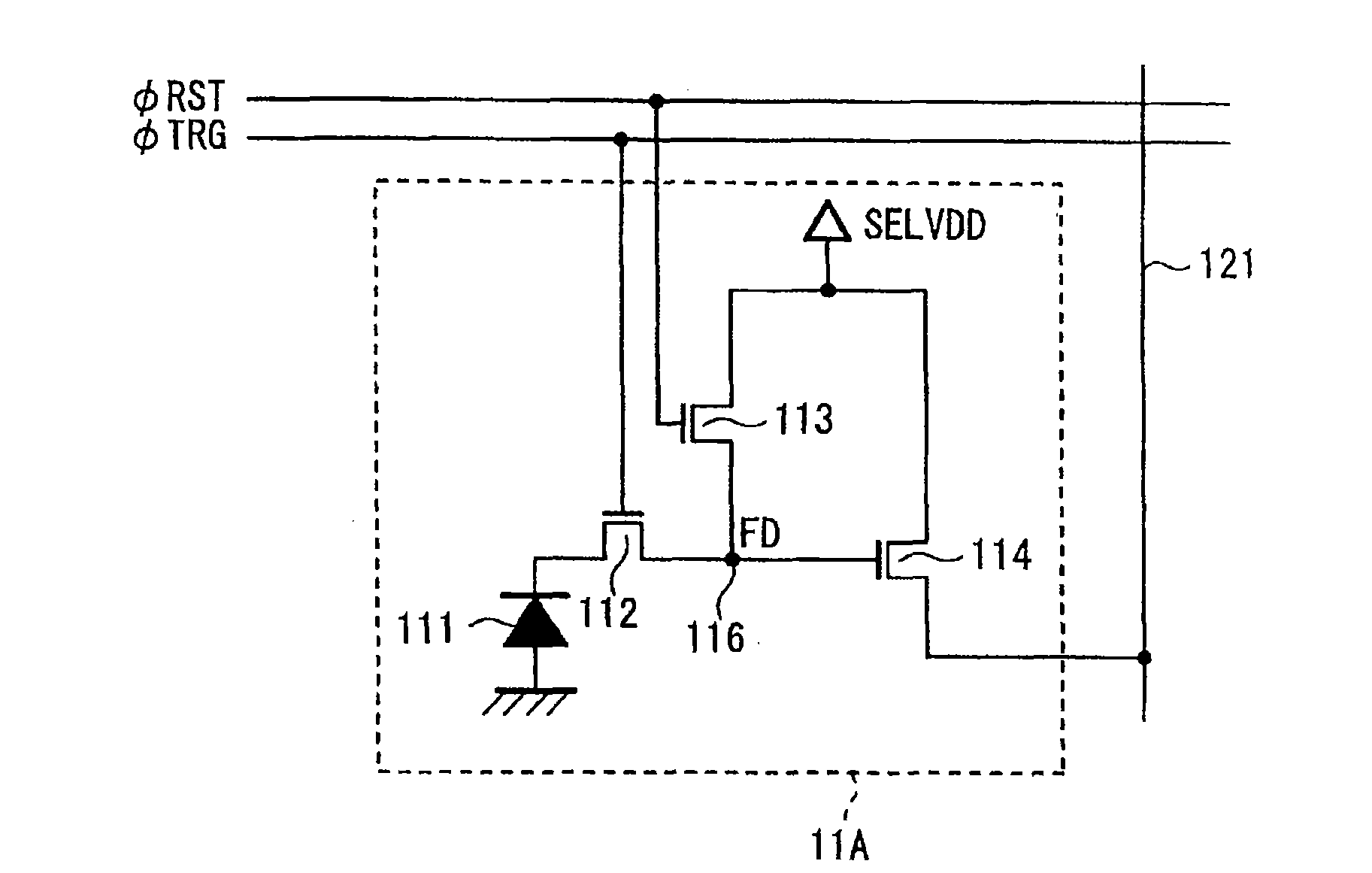
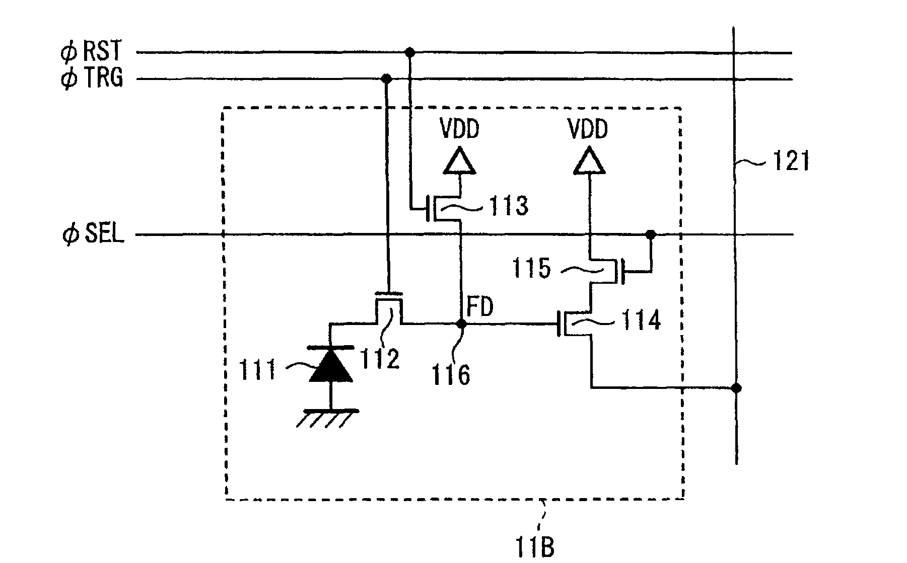
[0030] The conversion efficiency of photoelectric conversion in converting electric charge into signal voltage has been studied. Specifically, the photoelectrically converted charges are converted into voltages and output as pixel signals from circuits of the MOS image sensor. Therefore, even when the number of electrons (charge amount) per pixel is small, if the conversion efficiency of the signal voltage representing each charge is increased, the number reduction caused by the reduction in the area of the photodiode can be obtained compensate.
[0031] The conversion efficiency η is defined by the following equation (1). The unit is μV / e:
[0032] [equation 1]
[0033] η = q C FD G [ μV / e ]
[0034] q: amount of charge per electron
[0035] C FD : The total capacitance associated with the floating diffusion
[0...
PUM
 Abstract
Description
Claims
Application Information