Eureka AIR delivers breakthrough ideas for toughest innovation challenges, trusted by R&D personnel around the world.

Back-illuminated CMOS image sensor and manufacturing method thereof

A technology of an image sensor and a manufacturing method, applied in radiation control devices and other directions, to achieve the effects of suppressing noise and dark current, avoiding crosstalk, and improving quality

Active Publication Date: 2017-09-22
OMNIVISION TECH (SHANGHAI) CO LTD
View PDF5 Cites 4 Cited by
  • Summary
  • Abstract
  • Description
  • Claims
  • Application Information

AI Technical Summary

Problems solved by technology

[0006] The purpose of the present invention is to provide a back-illuminated CMOS image sensor and its manufacturing method, to solve the problem in the prior art that multiple photomasks are still needed to form structures such as metal pads after the pixel wafer and the logic wafer are bonded The problem

Method used


Image

  • Back-illuminated CMOS image sensor and manufacturing method thereof
  • Back-illuminated CMOS image sensor and manufacturing method thereof
  • Back-illuminated CMOS image sensor and manufacturing method thereof

Examples


Embodiment Construction

[0044] The back-illuminated CMOS image sensor proposed by the present invention and its manufacturing method will be further described in detail below with reference to the accompanying drawings and specific embodiments. Advantages and features of the present invention will be apparent from the following description and claims. It should be noted that all the drawings are in a very simplified form and use imprecise scales, and are only used to facilitate and clearly assist the purpose of illustrating the embodiments of the present invention.

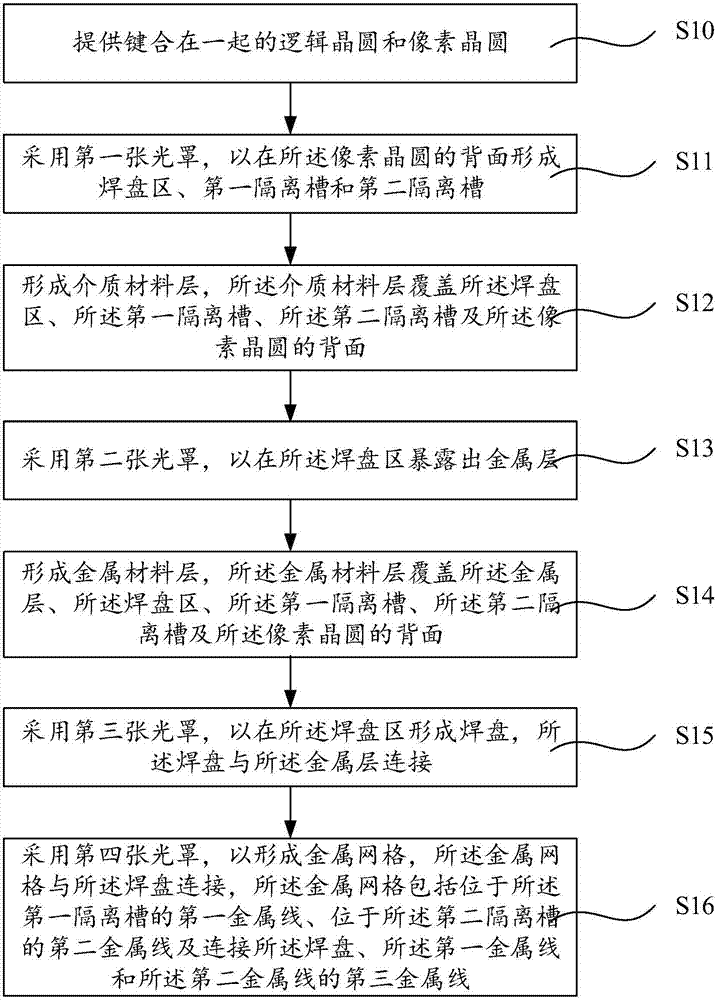
[0045] First, please refer to figure 1 , which is a schematic flowchart of a manufacturing method of a back-illuminated CMOS image sensor according to an embodiment of the present invention. Such asfigure 1 As shown, the manufacturing method of the back-illuminated CMOS image sensor includes:

[0046] Step S10: providing a logic wafer and a pixel wafer bonded together;

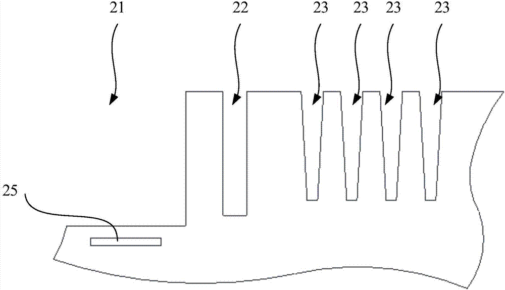
[0047] Step S11: using a first photomask to form a pad area, a f...


PUM


Abstract

The invention provides a back-illuminated CMOS image sensor and a manufacturing method thereof. The structure such as a bonding pad can be formed through the application of four photomasks, so that the application of the photomasks is reduced; and furthermore, a formed metal gridding is connected with the bonding pad, and comprises a first metal wire positioned in a first isolation groove, a second metal wire positioned in a second isolation groove, and a third metal wire for connecting the bonding pad, the first metal wire and the second metal wire, so that incident light can be preferably limited through the metal gridding, the appearance of crosstalk is avoided, and the quality of the back-illuminated CMOS image sensor is improved. Further, negative pressure is applied onto the bonding pad, so that the negative pressure is also applied onto the metal gridding connected with the bonding pad, namely the negative pressure is applied on a first isolation structure formed in the first isolation groove and a second isolation structure formed in the second isolation groove, and the generation of noisy points and dark current can be inhibited through the negative pressure applied onto the first isolation structure and the second isolation structure.

Description

technical field [0001] The invention relates to the technical field of image sensor manufacturing, in particular to a back-illuminated CMOS image sensor and a manufacturing method thereof. Background technique [0002] The image sensor is developed on the basis of photoelectric technology. The so-called image sensor is a sensor that can sense optical image information and convert it into an output signal. Image sensors can improve the visual range of the human eye, enabling people to see the microcosm and macrocosm that cannot be seen by the naked eye, see what happens in places that people cannot reach temporarily, and see various physical and chemical changes beyond the visual range of the naked eye. Life, physiology, the occurrence and development of disease, and so on. It can be seen that image sensors play a very important role in people's culture, sports, production, life and scientific research. It can be said that modern human activities can no longer be separated ...

Claims


Application Information

Patent Timeline
Patent Type & Authority Applications(China)
IPC IPC(8): H01L27/146
Inventor 邢家明高喜峰叶菁施喆天
Owner OMNIVISION TECH (SHANGHAI) CO LTD
Why Eureka
Eureka Blog
Learn More