Selective wave crest welding device and method

A wave soldering and selective technology, applied in auxiliary devices, measuring devices, welding equipment, etc., can solve the problems of reduced production efficiency, inability to know the welding quality in real time, increased labor costs, etc., and achieve the effect of improving the degree of automation

Pending Publication Date: 2018-03-06
深圳市阿拉玎光电自动化有限公司
View PDF10 Cites 3 Cited by
  • Summary
  • Abstract
  • Description
  • Claims
  • Application Information

AI Technical Summary

Problems solved by technology

[0003] The existing soldering process cannot immediately know the quality of the soldering during soldering, and can only use manual or machine detection of the quality information of each soldering point on the circuit board after all soldering points are soldered
This leads to an increase in labor costs and a reduction in production efficiency

Method used


Image

  • Selective wave crest welding device and method
  • Selective wave crest welding device and method
  • Selective wave crest welding device and method

Examples


Embodiment Construction

[0035] Below, the present invention will be further described in conjunction with the accompanying drawings and specific implementation methods. It should be noted that, under the premise of not conflicting, the various embodiments described below or the technical features can be combined arbitrarily to form new embodiments. .

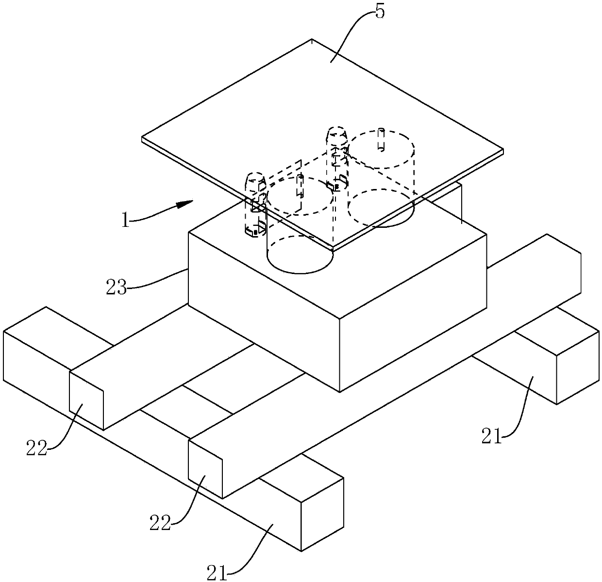
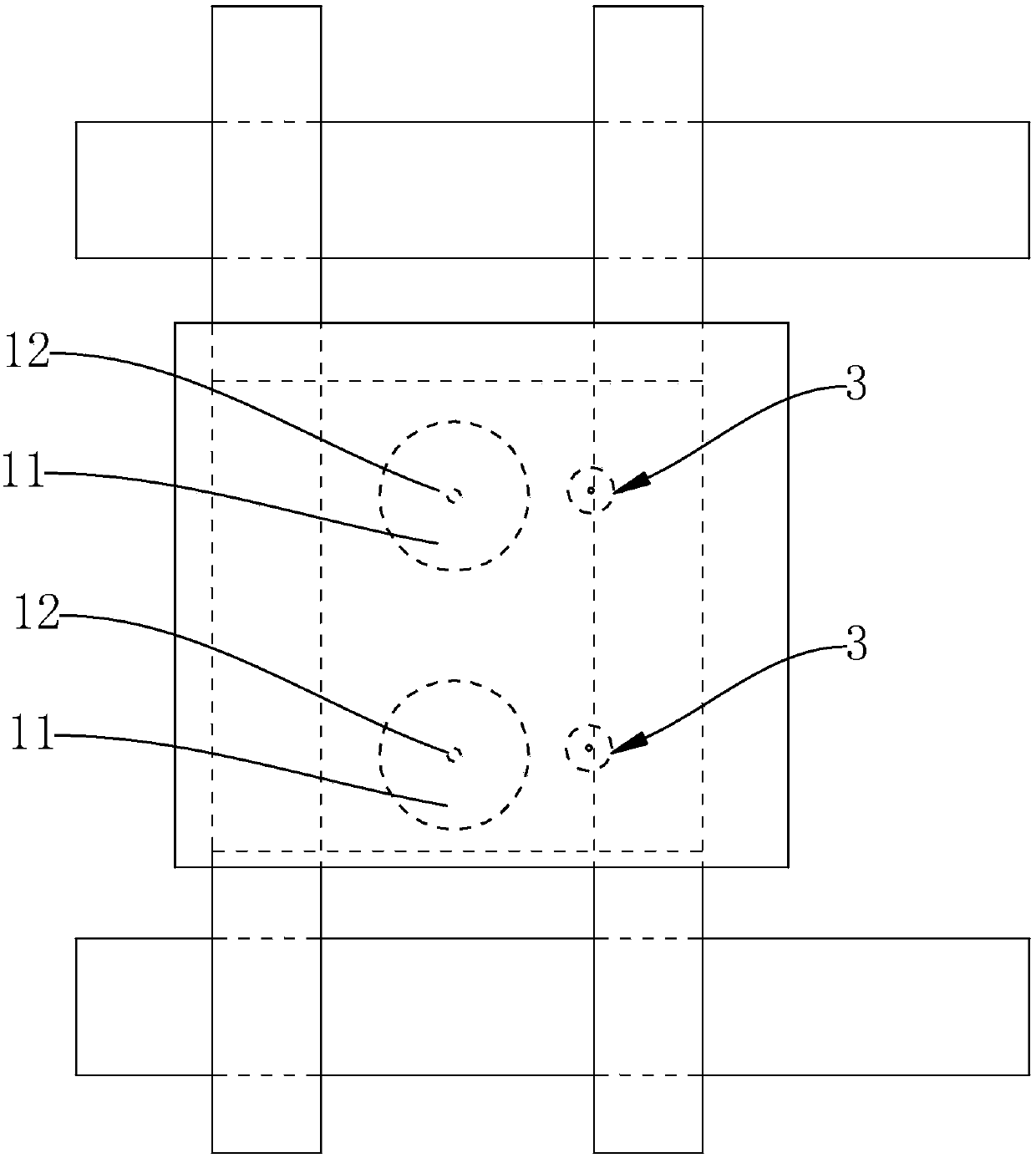
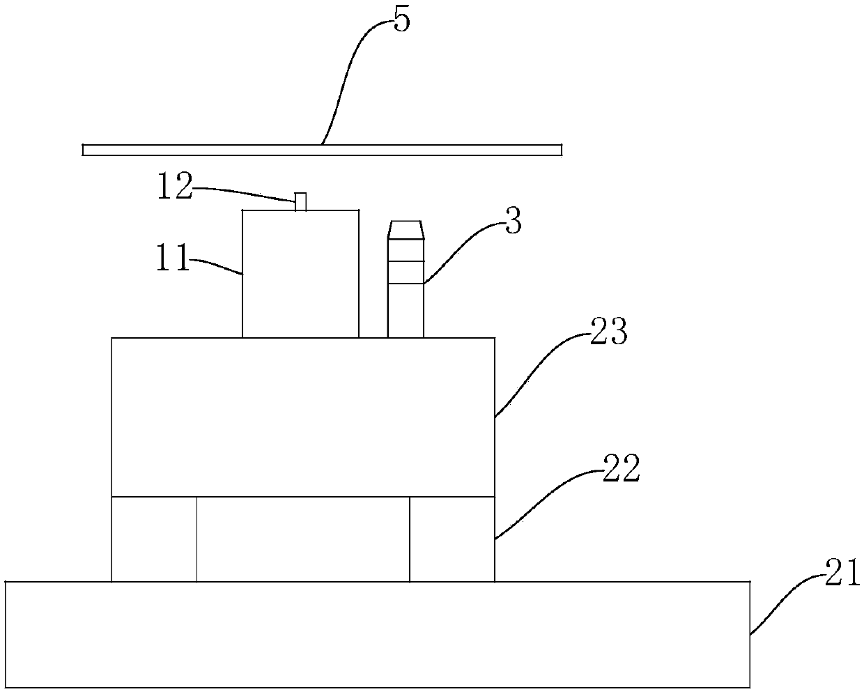
[0036] like Figure 1-4 As shown, the present invention provides a selective wave soldering device, including a soldering unit 1 , a driving unit 2 , an optical detection unit 3 and a control unit 4 . The soldering unit 1 is suitable for soldering a circuit board 5 . The driving unit 2 is used to drive the welding unit 1 to move, so as to realize the welding of various points on the circuit board 5 . The optical detection unit 3 is used to acquire images of the circuit board 5 and transmit the acquired images to the control unit 4 . The control unit 4 is respectively connected with the welding unit 1 , the driving unit 2 and the optical detection un...


PUM


Abstract

The invention discloses a selective wave crest welding device and method. The selective wave crest welding device comprises at least one welding unit applicable to welding a circuit board in a selective wave crest welding manner, a drive unit used for driving the welding unit to move in three-dimensional space, at least one optical detection unit used for obtaining an image of a welding point on the circuit board, and a control unit which is in signal connection with the welding unit, the drive unit and the optical detection unit. The control unit is suitable for controlling the drive unit tomove the welding unit to the preset position, the control unit is suitable for controlling the welding unit to spray welding fluid out to the circuit board so as to weld or maintain the circuit board,and the control unit is suitable for obtaining the image, obtained by the optical detection unit, of the welding point and processing the image so as to detect whether defects exist in the welding point.

Description

technical field [0001] The invention relates to manufacturing equipment in the electronics, circuit board and liquid crystal industries, in particular to a selective wave soldering device and a soldering method. Background technique [0002] At present, in the process of manufacturing printed circuit boards or liquid crystal screens, it is necessary to solder electronic components to the circuit boards with liquid tin. [0003] In the existing soldering process, the soldering quality cannot be known immediately during soldering, and the quality information of each soldering point on the circuit board can only be detected manually or by machine after all the soldering points are soldered. This has resulted in an increase in labor costs and a reduction in production efficiency. Contents of the invention [0004] In order to overcome the deficiencies in the prior art, one of the objects of the present invention is to provide a selective wave soldering device, which includes ...

Claims


Application Information

Patent Timeline
Patent Type & Authority Applications(China)
IPC IPC(8): B23K3/08G01N21/956
CPCG01N21/956B23K3/08H05K2203/044G01N2021/95646
Inventor 赖国荣刘绕兵朱德银
Owner 深圳市阿拉玎光电自动化有限公司
Why Eureka
Try Eureka