Integrated circuit board cutting device

A technology for integrated circuit boards and cutting devices, which is applied to fine working devices, grinding machines, metal processing equipment, etc., can solve the problems of low grinding efficiency, complicated cutting and processing of copper clad laminates, and reduce the processing efficiency of copper clad laminates. Processing efficiency, the effect of improving the speed of grinding

Active Publication Date: 2018-03-06
高唐融知融智科技服务有限公司
View PDF4 Cites 1 Cited by
  • Summary
  • Abstract
  • Description
  • Claims
  • Application Information

AI Technical Summary

Problems solved by technology

[0004] When the materials in the bonding sheet are metal plates and glass fiber cloth, after the copper clad laminate is cut, there are generally metal debris or glass fiber cloth debris left after cutting, metal debris or glass fiber cloth debris on the section of the copper clad laminate. Fiber cloth debris is easy to adhere to the corners of the copper clad laminate, and metal debris or glass fiber cloth debris is easy to scratch the surface of the copper clad laminate during the process of moving the copper clad laminate, resulting in poor color quality of the entire copper clad laminate; There are excess medium metal and glass fiber cloth at the corners of the cut copper clad laminate, so it is necessary to use a chamfering device to grind the multiple corners of the copper clad laminate separately, resulting in low grinding efficiency and reduced copper clad laminate. Processing efficiency; at the same time, it will cause metal debris or glass fiber cloth debris to be generated again on the copper clad laminate, and further cleaning of the metal debris or glass fiber cloth debris will be required, which will complicate the cutting and processing of the entire copper clad laminate, and increase the The probability of the surface of the copper clad laminate being scratched

Method used


Image

  • Integrated circuit board cutting device
  • Integrated circuit board cutting device

Examples


Embodiment Construction

[0023] Further detailed explanation through specific implementation mode below:

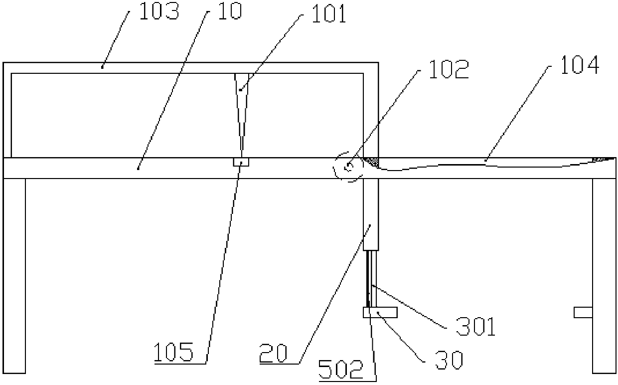
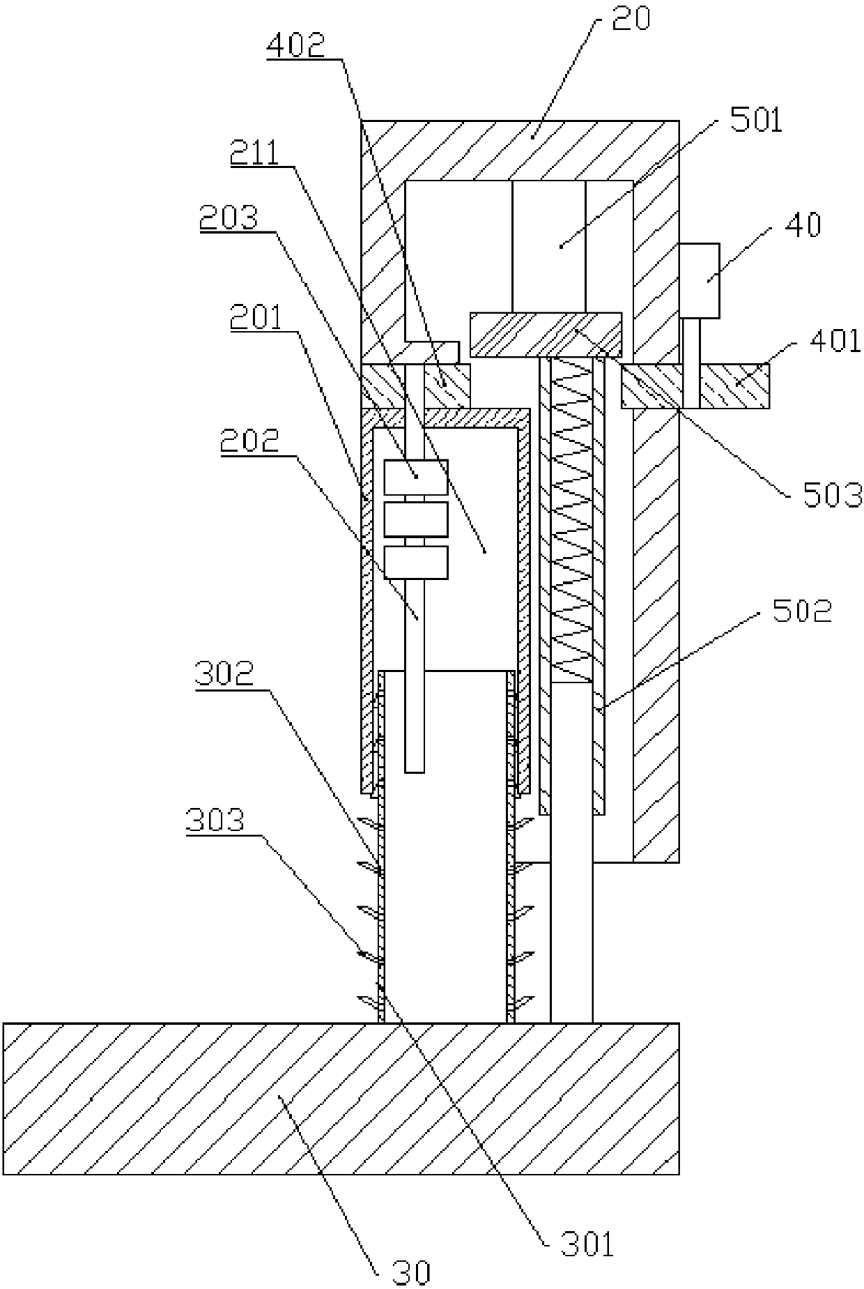
[0024] The reference signs in the accompanying drawings of the description include: cutting table 10, cutting knife 101, conveying roller 102, support frame 103, discharge channel 104, cutting groove 105, sleeve 20, grinding roller 201, accommodating cavity 211, rotating shaft 202 , fan blade 203, receiving plate 30, collecting tube 301, collecting hole 302, collecting plate 303, motor 40, driving gear 401, driven gear 402, first telescopic rod 501, second telescopic rod 502, transmission gear 503.

[0025] The embodiment is basically as attached figure 1 And attached figure 2 Shown: an integrated circuit board cutting device, including a cutting table 10, a cutting transmission mechanism and a grinding unit, one end of the cutting table 10 is provided with a vertical discharge channel 104, and the cross section of the discharge channel 104 is rectangular The corner grinding unit is welded on ...


PUM


Abstract

The invention relates to the field of a circuit board, in particular to an integrated circuit board cutting device. Four angle lapping units are arranged in the device, and the angle lapping units canconduct simultaneous lapping for four rim angles of a copper-clad plate. In the lapping process, a second telescopic rod can be stretched, further multiple copper-clad plates are stacked on a receiving plate, the rim angles of the copper-clad plates can be convenient for simultaneous lapping, and the lapping efficiency of the rim angles of the copper-clad plates can be further improved. Meanwhile, the stacked copper-clad plates do not need to be arranged again, and the subsequent processing for the copper-clad plates is convenient. The integrated circuit board cutting device can improve the lapping efficiency of the rim angles of the copper-clad plates.

Description

technical field [0001] The invention belongs to the field of circuit boards, in particular to an integrated circuit board cutting device. Background technique [0002] The Chinese name of PCB is printed circuit board, also known as printed circuit board. It is an important electronic component, a support for electronic components, and a carrier for electrical connections of electronic components. The processing process of the formed printed circuit board is complicated, including cutting, drilling, copper sinking, pattern transfer, pattern electroplating, stripping, etching, green oil, characters, gold-plated fingers, forming, testing and final inspection. Processing steps, each step also includes several small processing steps, such as the cutting step, the specific processing is to cut the copper clad laminate, the cutting step can make the size of the copper clad laminate and the processed printing The size of the circuit board is suitable, and then the cut copper clad l...

Claims


Application Information

Patent Timeline
Patent Type & Authority Applications(China)
IPC IPC(8): B28D5/04B24B9/02
CPCB24B9/02B28D5/04
Inventor 胡红生
Owner 高唐融知融智科技服务有限公司
Why Eureka
Try Eureka