Circuit board line compensation method and device

A technology of circuit board circuit and compensation method, which is applied in the direction of printed circuit, printed circuit manufacturing, and chemical/electrolytic method to remove conductive materials, etc., can solve the problems of inability to achieve fine correction, heavy workload, etc., and improve the production quality efficiency and quality assurance

Active Publication Date: 2018-03-09
深圳嘉立创科技集团股份有限公司
View PDF3 Cites 6 Cited by
  • Summary
  • Abstract
  • Description
  • Claims
  • Application Information

AI Technical Summary

Problems solved by technology

However, the general modification of circuit etching process parameters must be done manually, the workload is heavy, and the goal of fine modification cannot be achieved

Method used


Image

  • Circuit board line compensation method and device
  • Circuit board line compensation method and device
  • Circuit board line compensation method and device

Examples


Embodiment Construction

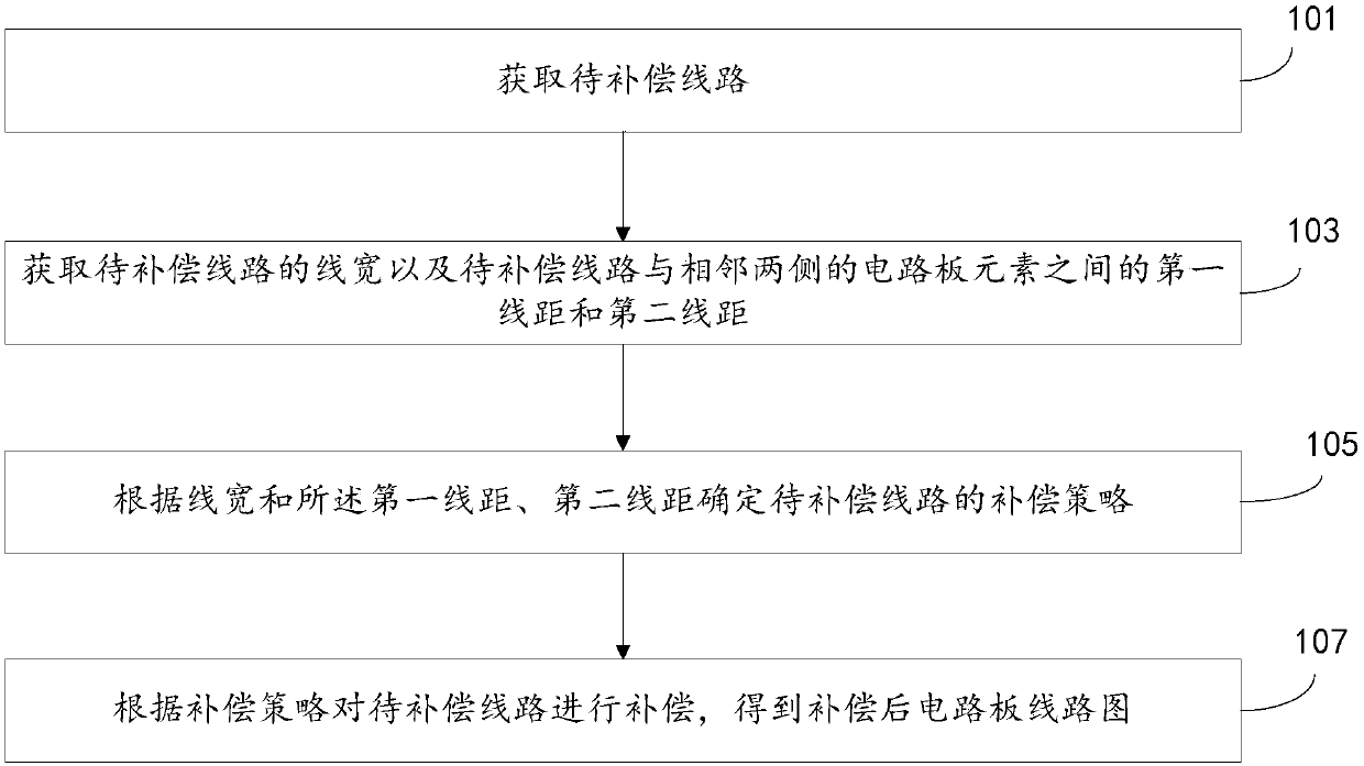
[0022] In order to make the object, technical solution and advantages of the present invention clearer, the present invention will be further described in detail below in conjunction with the accompanying drawings and embodiments. It should be understood that the specific embodiments described here are only used to explain the present invention, not to limit the present invention.

[0023] Unless otherwise defined, all technical and scientific terms used herein have the same meaning as commonly understood by one of ordinary skill in the technical field of the invention. The terms used herein in the description of the present invention are for the purpose of describing specific embodiments only, and are not intended to limit the present invention. As used herein, the term "and / or" includes any and all combinations of one or more of the associated listed items.

[0024] In order to ensure the production of fine lines on current printed circuit boards, an embodiment of the prese...


PUM


Abstract

The invention relates to a circuit board line compensation method. A to-be-compensated line is acquired; a line width of the to-be-compensated line and a first line distance and a second line distancebetween the to-be-compensated line and circuit board elements at two adjacent sides are acquired; the compensation strategy of the to-be-compensated line is determined according to the line width, the first line distance and the second line distance; the to-be-compensated line is compensated according to the compensation strategy to acquire a compensated circuit board line diagram. The inventionfurther provides a circuit board circuit line compensation device. Through acquiring the line width and the line distances of the to-be-compensated line, the compensation strategy suitable for the to-be-compensated line is determined, the compensated circuit board line diagram is formed, so that the manufacturing process of circuit boards can be controlled according to design parameters of the compensated circuit board line diagram.

Description

technical field [0001] The invention relates to the field of circuit board production, in particular to a circuit board line compensation method and a circuit board line compensation device using the circuit board line compensation method. Background technique [0002] A printed circuit board (Printed Circuit Board, PCB) is a selective arrangement of conductive patterns and vias on the insulating board base material according to the pre-design, so as to realize the transmission of signals between board layers. Made by exposure, development, etching, gold plating and other processes. In recent years, as the functions of various portable consumer electronic products continue to increase, and the volume requirements are getting smaller and smaller, it is inevitable that the PCB board carrying electronic components will also rapidly develop towards light, thin, short, miniaturized, high-density interconnected PCB (High Density Interconnection, HDI) applications are becoming mor...

Claims


Application Information

Patent Timeline
Patent Type & Authority Applications(China)
IPC IPC(8): H05K3/06
CPCH05K3/061H05K3/068H05K2203/0502
Inventor 许明灯高楚涛
Owner 深圳嘉立创科技集团股份有限公司
Why Eureka
Try Eureka