Circuit structure manufacturing method and circuit structure

A technology of circuit structure and manufacturing method, which is applied in the direction of printed circuit manufacturing, printed circuit, printed circuit components, etc., can solve the problems of increasing the difficulty of chemical surface adjustment treatment, the inability to form large differences in properties, and easy occurrence of overflow plating, etc. Achieve the effects of reducing the influence of crystal structure and appearance, large operating window, and cost saving

Inactive Publication Date: 2018-03-20
SHANGHAI AMPHENOL AIRWAVE COMM ELECTRONICS CO LTD
View PDF6 Cites 2 Cited by
  • Summary
  • Abstract
  • Description
  • Claims
  • Application Information

AI Technical Summary

Problems solved by technology

The disadvantage of this solution is that due to the roughness of the product surface formed by non-metallic materials, after electromagnetic irradiation, the properties of the irradiated surface and the non-irradiated surface cannot form a large difference, which increases the difficulty of chemical surface adjustment and treatment, and is prone to overflow plating

Method used


Image

  • Circuit structure manufacturing method and circuit structure
  • Circuit structure manufacturing method and circuit structure
  • Circuit structure manufacturing method and circuit structure

Examples


Embodiment Construction

[0052] In order to make the above objects, features and advantages of the present invention more comprehensible, specific implementations of the present invention will be described in detail below in conjunction with the accompanying drawings.

[0053] In the following description, numerous specific details are set forth in order to provide a thorough understanding of the present invention. However, the present invention can be implemented in many other ways different from those described here, and those skilled in the art can make similar extensions without violating the connotation of the present invention, so the present invention is not limited by the specific implementations disclosed below.

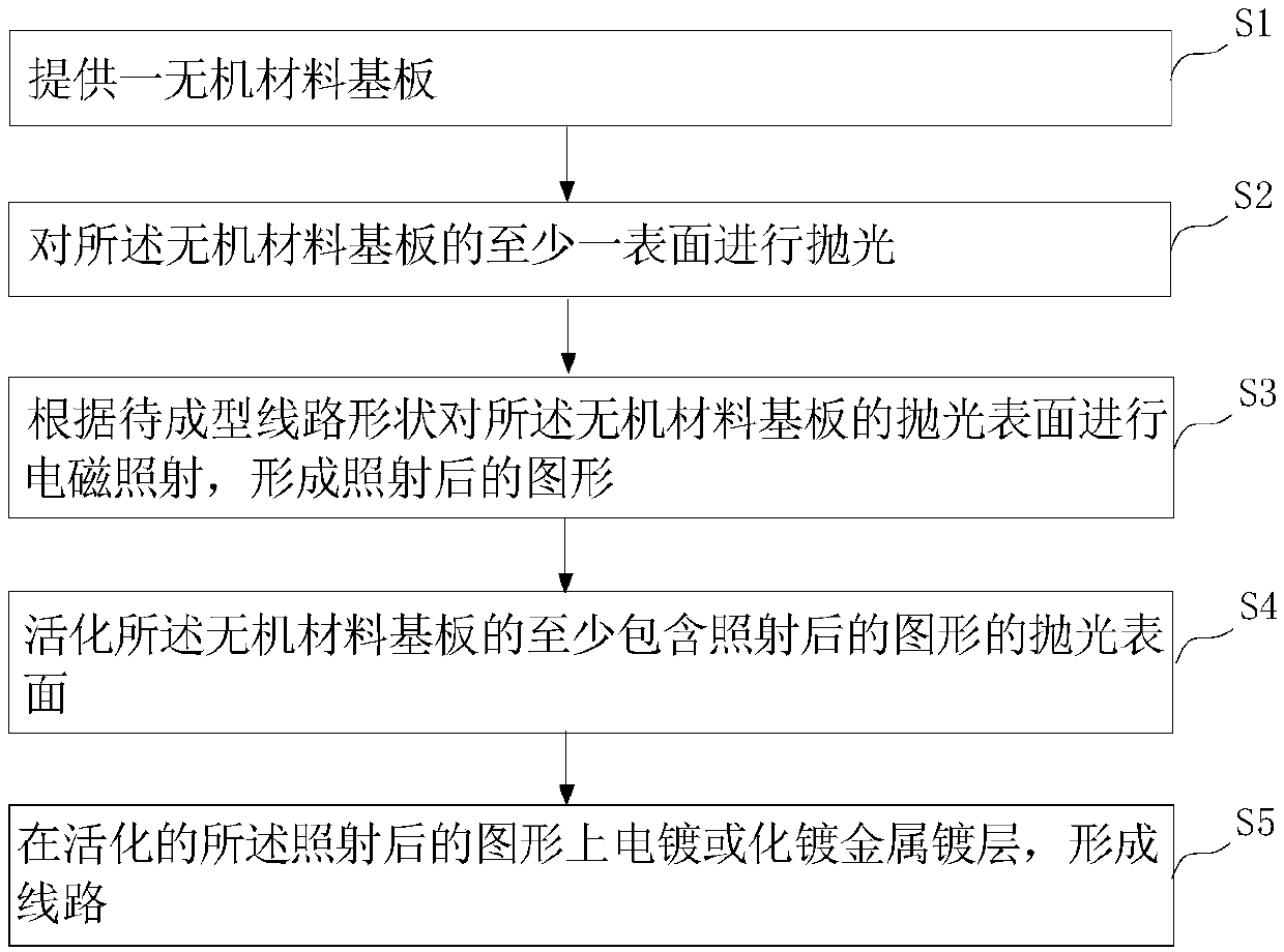
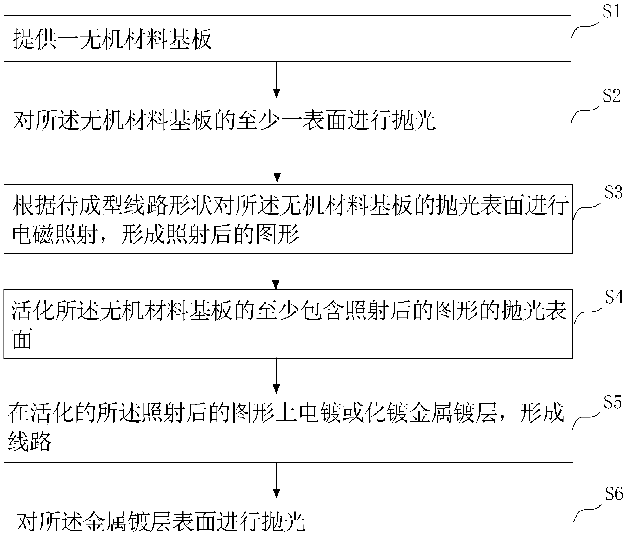
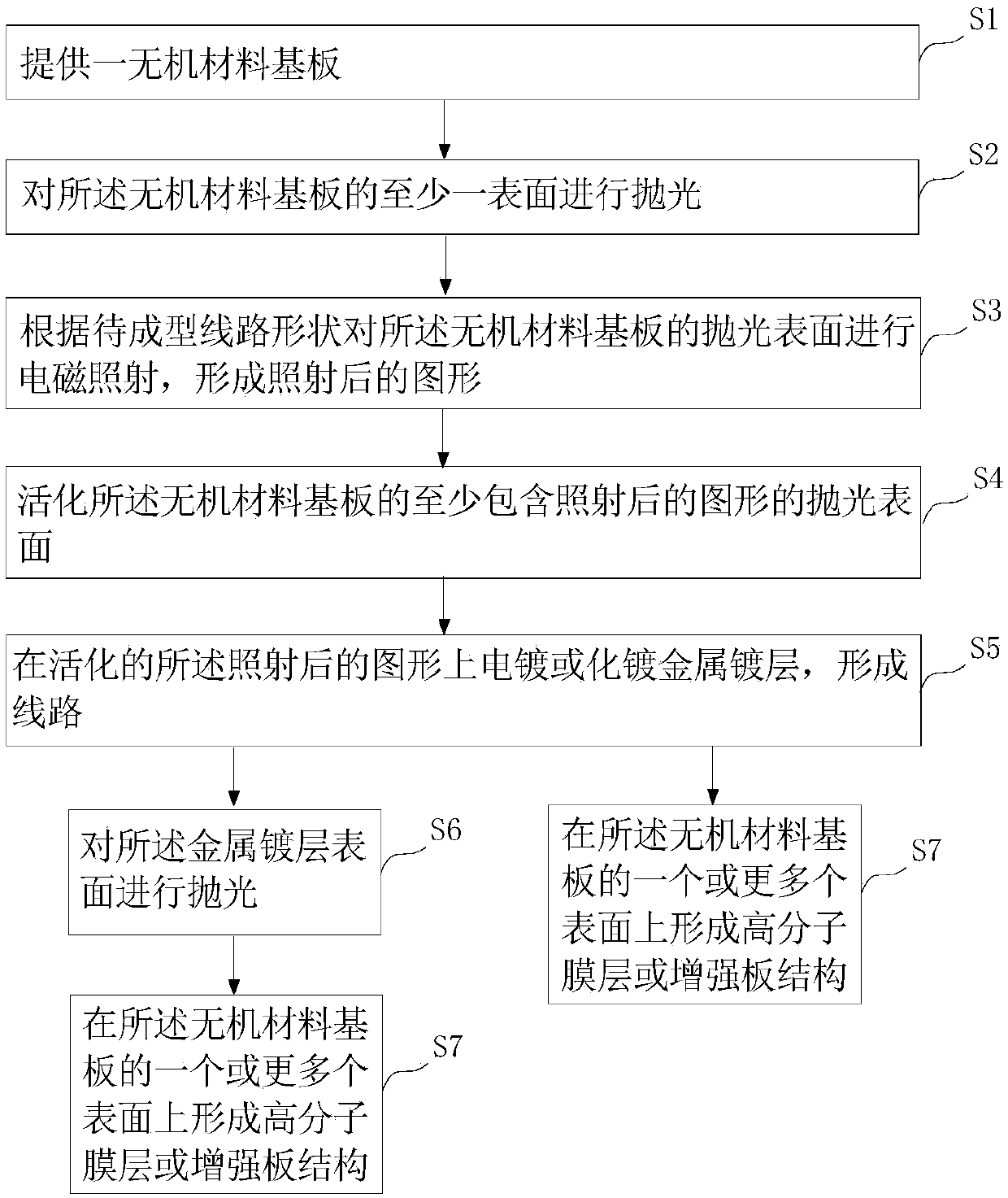
[0054] see figure 1 , in one embodiment, the circuit structure fabrication method comprises the following steps:

[0055] S1: providing an inorganic material substrate;

[0056] S2: Polish at least one surface of the inorganic material substrate; since the inorganic material has a...


PUM

PropertyMeasurementUnit
surface roughnessaaaaaaaaaa

Abstract

The invention provides a circuit structure manufacturing method and a circuit structure. The method comprises the following steps: S1, providing an inorganic material substrate; S2, polishing at leastone surface of the inorganic material substrate; S3, carrying out electromagnetic irradiation on a polished surface of the inorganic material substrate according to the shape of a circuit to be formed so as to form an irradiated pattern; S4, activating the polished surface, at least containing the irradiated pattern, of the inorganic material substrate; and S5, electroplating or chemically plating a metal clad layer on the activated irradiated pattern so as to form the circuit. According to the circuit structure manufacturing method and the circuit structure provided by the invention, a metalcompound or a metal media does not need to be used, the yield is high, and the circuit performance is good.

Description

technical field [0001] The invention relates to the technical field of electronic circuits, in particular to a method for manufacturing a circuit structure and a circuit structure. Background technique [0002] The current three-dimensional circuit manufacturing methods are mainly laser direct structure (LDS) and chemical plating after laser activation of ordinary plastics. Applicable substrates are relatively limited, usually plastic substrates, not suitable for inorganic materials such as ceramics and glass. [0003] Due to its high hardness and beautiful appearance, industrial glass is also widely used in electronic terminal equipment. Similarly, ceramics are gradually being used in electronic terminal equipment, such as mobile phone casings. Industrial ceramics use artificial compounds such as alumina, magnesia, zirconia, lead oxide, titanium oxide, silicon carbide, boron carbide, silicon nitride, and boron nitride as raw materials, and are crushed, formed, and manufac...

Claims


Application Information

Patent Timeline
Patent Type & Authority Applications(China)
IPC IPC(8): H05K1/11H05K3/18
CPCH05K1/11H05K3/18H05K2203/0307
Inventor 陈进陈德智蒋海英
Owner SHANGHAI AMPHENOL AIRWAVE COMM ELECTRONICS CO LTD
Why Eureka
Try Eureka