Check patentability & draft patents in minutes with Patsnap Eureka AI!

Chip batch production testing system

A test system and chip technology, applied in automated test systems, electronic circuit tests, etc., can solve problems such as inconvenient analysis, increased chip test costs, lack of data log information, etc., to achieve convenient online debugging and save chip mass production test costs , The effect of shortening the development time

Active Publication Date: 2018-03-23
XIAN INTELLIGENCE SILICON TECH INC
View PDF6 Cites 4 Cited by
  • Summary
  • Abstract
  • Description
  • Claims
  • Application Information

AI Technical Summary

Problems solved by technology

To complete the configuration test of the test stimulus on the tester side, a high-end tester with a large vector depth is required to complete the test, which will increase the test cost of the chip; while using the SLT test, the test stimulus is generated by the system chip on the test board, which not only saves Storage of test vectors and providing a high-frequency test environment, but the SLT test loses the precise DC parameters and timing parameters of the test machine, and lacks data log information, which is not convenient for subsequent analysis

Method used


Image

  • Chip batch production testing system
  • Chip batch production testing system
  • Chip batch production testing system

Examples


Embodiment 1

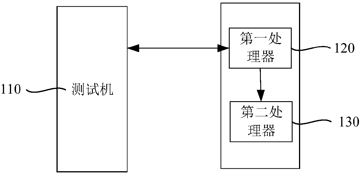
[0033] See figure 1 , figure 1 It is a schematic diagram of a chip mass production testing system provided by an embodiment of the present invention. Specifically, the testing system may include: a testing machine 110; a first processor 120, electrically connected to the testing machine 110, configured to receive control instructions of the testing machine 110, configure the chip to be tested according to the control instructions and The configuration result is sent to the testing machine 110; the second processor 130 is electrically connected to the first processor 120 for configuring and testing the chip under test according to the test vector file sent by the first processor 120 ;

[0034] Wherein, the testing machine 110 is used to complete the test of the first test vector of the chip under test, and the test machine 110 cooperates with the first processor 120 to complete the second test vector of the chip under test The first processor 120 cooperates with the second p...

Embodiment 2

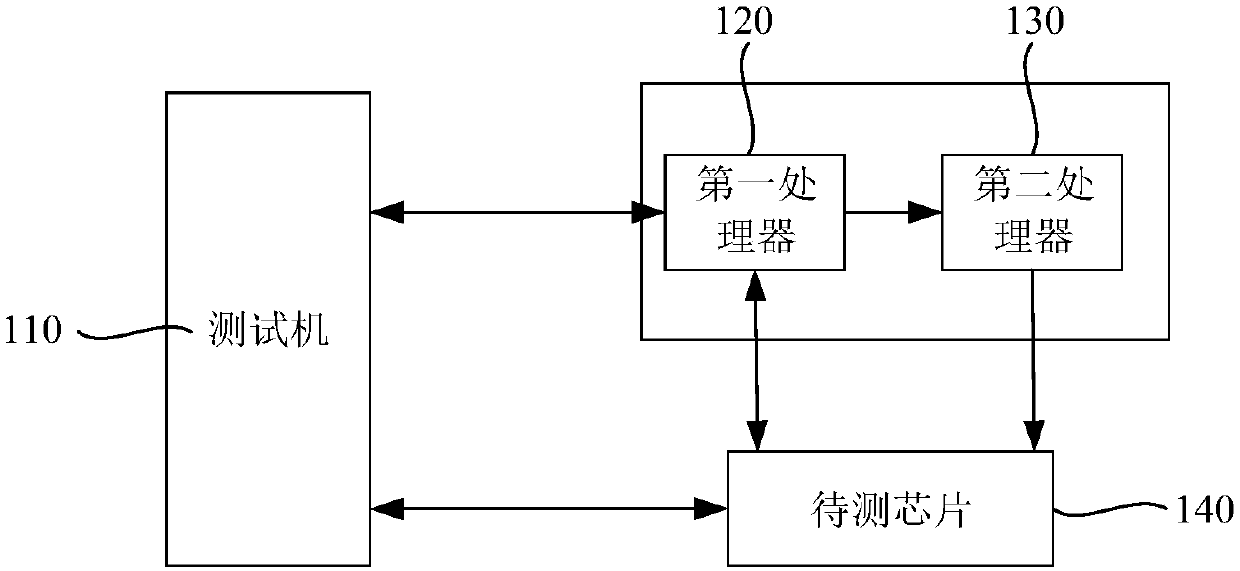
[0047] See figure 2 , figure 2It is a schematic diagram of another chip mass production testing system provided by the embodiment of the present invention. This embodiment introduces the test system proposed by the present invention in detail on the basis of the above embodiments. The testing system includes a testing machine 110 , a first processor 120 and a second processor 130 . The first processor 120 is electrically connected to the testing machine 110 and receives control instructions sent by the testing machine 110 . The second processor 130 is electrically connected to the first processor 120 and receives data information sent by the first processor 120 . Testing machine 110 carries out some direct current (Direct Current, be called for short DC), alternating current (Alternative Current, be called for short AC) parameter test of chip 140 to be tested, wherein, testing machine 110 alone completes the test of open short circuit, leakage current and quiescent working...

Embodiment 3

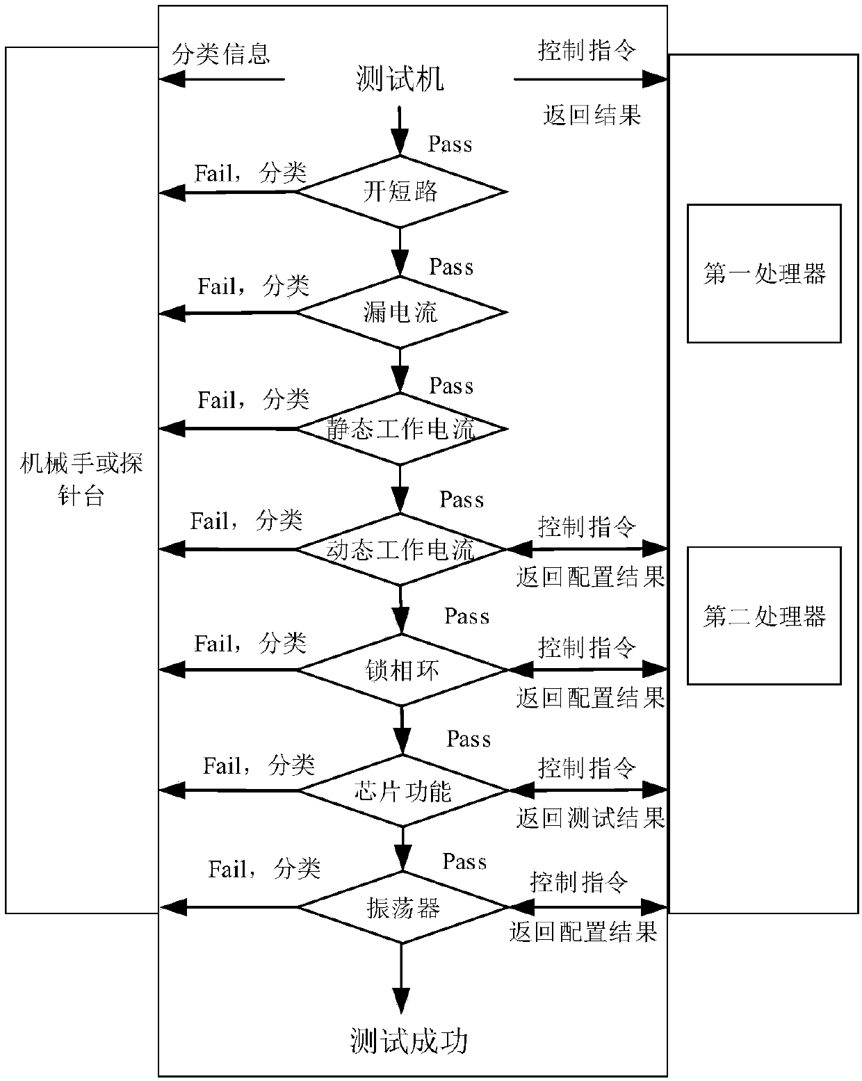
[0050] See Figure 3a ~ Figure 3b , Figure 3a A schematic flow chart of a chip mass production testing method provided by an embodiment of the present invention; Figure 3b It is a schematic flowchart of another chip mass production testing method provided by the embodiment of the present invention. This embodiment describes in detail the actual workflow of the testing method proposed by the present invention on the basis of the above embodiments. details as follows:


PUM


Abstract

The invention relates to a chip batch production testing system comprising the following units: a tester 110; the first processor 120 electrically connected with the tester 110 and used for receivinga control order from the tester, configuring a to-be-tested chip according to the control order, and sending the configuration result to the tester 110; the second processor 130 electrically connectedwith the first processor 120 and used for testing the to-be-tested chip according to a testing excitation file sent by the first processor 120. The testing system can finish different test vectors through cooperation of the tester, the first processor and the second processor, thus finishing a batch production test of a complex chip on a low end testing platform, saving the chip batch productiontesting cost, and greatly reducing the testing program developing time; the testing system is convenient in online debug.

Description

technical field [0001] The invention belongs to the technical field of chip testing, and in particular relates to a chip mass production testing system. Background technique [0002] FPGA (Field Programmable Gate Array, referred to as FPGA), that is, field programmable gate array. FPGA and Chengdu are high and small in size, and have the function of realizing special applications through user programming. FPGA can not only solve the shortage of customized circuits, but also overcome the shortcomings of the limited number of gate circuits of the original programmable devices. It is one of the most dynamic and promising technologies in the field of electronic design. [0003] With the wide application of FPGA, its reliability becomes more and more prominent, so the test demand for FPGA becomes particularly urgent. Testing is the most expensive and difficult part of design, and testing will have an increasing impact on product launch time and development cycle. Testing has b...

Claims


Application Information

Patent Timeline
IPC IPC(8): G01R31/28
CPCG01R31/2834
Inventor 孙浩涛田军贾红程显志陈维新韦嶔
Owner XIAN INTELLIGENCE SILICON TECH INC
Features
  • R&D
  • Intellectual Property
  • Life Sciences
  • Materials
  • Tech Scout
  • Unparalleled Data Quality
  • Higher Quality Content
  • 60% Fewer Hallucinations
Learn More